Researchers based in China, Singapore and Turkey have used an extremely thin layer of silicon dioxide (SiO2) insulator as a charge inverter in indium gallium nitride (InGaN) light-emitting diodes (LEDs), improving light output power and external quantum efficiency (EQE) [Zi-Hui Zhang et al, Appl. Phys. Lett., vol108, p133502, 2016].
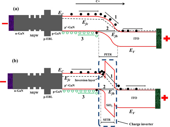
The aim of the SiO2 charge inversion layer is to improve hole injection past the electron-blocking layer (EBL) into the multiple quantum well (MQW) active light-emitting region (Figure 1). Poor hole injection is an undesirable feature of InGaN LEDs due to the low ionization of the magnesium doping that is used to create p-type GaN. The knock-on effect is that hole injection into InGaN MQWs is restricted to a couple of wells at the p-GaN end.

Figure 1: Schematic energy band diagrams (layer thickness not to scale) for (a) device A without SiO2 charge inverter and (b) device B with charge inverter. Carrier transport processes: 1. non-equilibrium electrons (solid circles) travel to the ITO layer from the conduction band of the p+-GaN layer; 2. electron interband tunneling simultaneously produces holes (open circles), and holes then travel (3) to MQW region. EC conduction and EV valence bands. Efe electron and Efh hole quasi-Fermi levels.
Further, since there are few holes in the MQW region, electrons tend to overshoot, ending up in the p-GaN contact where non-radiative recombination is more likely. Aluminium gallium nitride (AlGaN) electron-blocking layers are used to avoid this, but these layers also unfortunately inhibit hole injection.
The proposed effect of the thin layer of SiO2 insulator is to reduce the thickness of the barrier for electrons to be removed from the valence band of the p-type GaN layer of the LEDs into the conduction band of the indium tin oxide (ITO) transparent current-spreading layer.
Simulations suggest that the SiO2 forms a weak inversion layer on the p-GaN side where electrons accumulate. The researchers from Hebei University of Technology in China, Nanyang Technological University in Singapore, Bilkent University in Turkey, and South University of Science and Technology in China, explain: "The inversion layer is able to attract and confine the electrons at the p+-GaN/insulator interface. This can then substantially shorten the width of the tunnel region, which can significantly increase the carrier tunnel efficiency."
The simulations suggest that the tunneling width of ~3.5nm without SiO2 can be reduced to ~2nm by the thin insulator layer.
Another effect of the SiO2 is to increase the magnitude of the electric field in the tunneling region due to the lower dielectric constant of SiO2 (3.9) relative to GaN (8.9), giving smoother, more effective hole transport from better tunneling. With better removal of electrons into the ITO layer under forward bias, there are more holes available for injection into the MQW.
The team also suggests that the SiO2 charge inverter structure could provide an easy way to enhance hole injection and quantum efficiency in ultraviolet (UV) LEDs with p-AlGaN hole injection layers. According to the researchers, a p+-AlGaN layer would have an even larger surface depletion region with improved tunneling of valence-band electrons into ITO.
The epitaxial material for the LEDs was grown by metal-organic chemical vapor deposition (MOCVD) on [0001] sapphire: 20nm GaN nucleation, 4μm GaN buffer, 2μm silicon-doped GaN, five-period 3nm/12nm In0.15Ga0.85N/GaN MQW, 25nm magnesium-doped p-Al0.20Ga0.80N EBL, 0.2μm magnesium-doped p-GaN hole source, and 20nm heavily magnesium-doped p+-GaN ohmic contact. The complete epitaxial wafer was annealed at 700°C in situ for 10 minutes in nitrogen.
The LED wafers were processed into 350μmx350μm mesas with ~1nm plasma-enhanced chemical vapor deposition (PECVD) silicon dioxide and 50nm ITO transparent conductor on the p+-GaN ohmic contact. LEDs without the extremely thin SiO2 layer were also produced. The thinness of the SiO2 was enabled by the less than 1nm root-mean-square roughness measured by atomic force microscopy (AFM) over a 1μmx1μm field on the p+-GaN surface.
The ITO layers of both device types were annealed at 630°C for a minute in a nitrogen/oxygen mix. The researchers believe that the final devices could be further improved by optimizing this step. The p- and n-contact metals were titanium/gold.

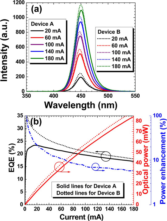
Figure 2: Experimentally measured (a) electroluminescence spectra, (b) EQE, optical power and power enhancement at different injection current levels for devices A and B.
One effect of the SiO2 layer was to reduced the forward voltage of the LEDs, due to improved hole injection according to the researchers. The light output was also increased with SiO2 layer across the current injection range (Figure 2). The spectral peaks of both device types first underwent a blue-shift associated with charge polarization screening and then red-shift at higher currents due to self-heating effects.
At 20mA, the external quantum efficiency (EQE) for the LED B with SiO2 layer was 20% greater than the value for LED A without. However, the efficiency enhancement fell to 10% at 180mA.
The higher EQE peak for device B also implies a larger droop: 48.6% at 100mA, compared with 27.6% for LED A. The researchers comment: "The observed efficiency droop for device B is likely due to the electron leakage caused by the inversion layer at the p+-GaN/SiO2 interface, given that more non-equilibrium holes are produced at the p+-GaN/SiO2 interface and the inversion layer occurs, which attracts more electrons to bypass the MQW region. Thus, more efforts are necessary to optimize the electron injection layer and/or the p-EBL so that both efficiency enhancement and reduced efficiency droop can be obtained."