Researchers in the USA have developed radio frequency switches based on nitride semiconductor voltage-controlled capacitors (varactors) [F. Jahan et al, IEEE Electron Device Letters, 9 January 2013]. The team, consisting of engineers from University of South Carolina (USC), Sensor Electronic Technology Inc (SET), Rensselaer Polytechnic Institute (RPI), writes: “The demonstrated switch is fully compatible with III-nitride heterostructure field-effect transistors (HFETs) or metal-insulator-semiconductor HFETs (MISHFETs) and has a great potential for high-performance monolithic microwave integrated circuits (MMICs).”
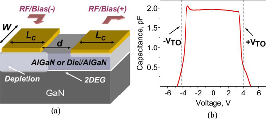
The varactors consisted of two Schottky contacts deposited over an aluminium gallium nitride on gallium nitride (AlGaN/GaN) heterostructure (Figure 1). The electrodes give capacitively coupled contacts (C3) with the two-dimensional electron gas (2DEG) that forms near the AlGaN/GaN interface. By biasing the varactor, a low capacitance results that blocks RF signals.

Figure 1: (a) C3 varactor layout. (b) C–V characteristic.
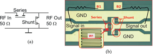
According to USC professor Grigory Simin, the purpose of the work was to demonstrate the potential of the C3 varactor and its advantages over FETs in RF switching applications. Two C3 varactors created a switch circuit in a coplanar waveguide (CPW) layout (Figure 2).

Figure 2: (a) Series–shunt MMIC layout. (b) RF switch image with multi-finger C3 region zoomed in.
The epitaxial structure (Figure 1) was grown on sapphire using metal-organic chemical vapor deposition (MOCVD). The semi-insulating GaN buffer layer was 1.5μm and the Al0.25Ga0.75N barrier was 20nm. The resulting 2DEG at the AlGaN/GaN interface had a sheet resistance of 300Ω/square.
The device mesa was formed using reactive ion etch (RIE). The metals used for the CPW and C3 varactor were nickel/gold. The nickel/gold combination gives a Schottky junction with the AlGaN layer. Plasma-enhanced chemical vapor deposition (PECVD) of 10nm silicon nitride passivated the surface of the device.
The device realized a series-shunt switch circuit (Figure 2). The switching was achieved by biasing through 2.5–5kΩ resistors that consisted of 3μm-wide 2–3mm-long meanders of 30nm-thick chromium with two bias terminals (B1 and B2).
A bias voltage of 30V was used to avoid the RF signal from accidentally switching the varactors. At 30V bias, the leakage was 2–10μA. The on-state consisted of both bias electrodes at 30V – the series varactor was then unbiased (on-state) and the shunt was biased (off-state). In the off-state, the output line bias was set to 0V – the series varactor was then biased (off-state) and the shunt unbiased (on-state).
Small inductances were introduced in the circuit by narrowing the signal lines and increasing the gap in the CPW pattern. The aim of this was to compensate for the capacitive component of the C3 varactor impedances.
The on-state insertion loss of the switch was less than 1.2dB over the range 4–20GHz. At 18GHz, the insertion loss is 0.8dB. The researchers compare this insertion loss with that obtained at similar frequencies using HFETs (1.5dB) and ferrite varactors (2dB). However, the insertion loss was more than expected from simulations. The researchers suggest that this could have been due to “imperfect capacitance compensation by the CPW inductance”.
The isolation provided by the switch in the off-state was ~25dB over a broad range of frequencies. At 18GHz this increased to 28dB.


