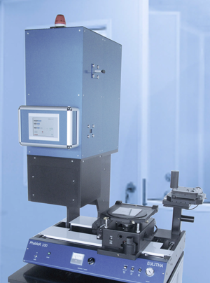
Eulitha AG of Würenlingen, Switzerland (a spin-off of the Paul Scherrer Institute in Villigen that offers nano-lithographic equipment and services for photonics and optoelectronic applications) says that one of its PhableR 100 photolithography systems has been installed at the UK's University of Bath.
The PhableR 100 exposure tool incorporates Eulitha's proprietary Displacement Talbot Lithography technology, which enables robust printing of very high-resolution periodic patterns at low cost. The system was purchased by the university as part of a comprehensive research program designed to develop manufacturing techniques for nano-engineered semiconductors, particularly gallium nitride (GaN).

Picture: Eulitha's PhableR 100 nano-lithography system.
The system's purchase was made possible following the award of a 5-year, £2.7m grant from the UK Engineering & Physical Sciences Research Council (EPSRC) as part of the council's Manufacturing of Advanced Functional Materials funding program.
The university has been active in GaN research since 1999 and has a reputation for combining nanofabrication techniques with semiconductor growth in order to improve the performance of optoelectronic devices such as light-emitting diodes.
Specifically, creating three-dimensional structures at the nanoscale provides a route to improving the quality of these materials and in turn the performance of devices. This should ultimately increase the energy efficiency in these and other emerging applications, such as water purification, where ultra-violet LEDs are used to prevent viruses reproducing.
As a result of the EPSRC investment, researchers in the Department of Electronic & Electrical Engineering now have access to a new nanolithography suite within the David Bullet Nanofabrication Cleanroom, of which the PhableR system forms part, alongside the existing access to crystal growth reactors and more conventional fabrication facilities.
The PhableR 100 system was chosen as it offers what is claimed to be the unique capability to pattern large areas up to 100mm in diameter with high fidelity in a very simple way. Its capability will be compared with another low-cost patterning technique, nanoimprint lithography, as part of the research.
"Initial results from the tool have matched and even exceeded our expectations," comments lead researcher Dr Philip Shields (lecturer in the Department of Electronic and Electrical Engineering). "There has been a lot of interest from other researchers to use the tool, and we look forward to developing new research collaborations as a consequence," he adds.
"Their research program focuses on manufacturing technologies for nano-engineered semiconductors which is an area where our innovative technologies have the potential to make a significant impact," says Eulitha's CEO Dr Harun Solak about the University of Bath.
The PhableR 100 system is capable of exposing periodic patterns down to feature sizes below 150nm, which rivals more expensive high-end i-line steppers. The patented focus-free imaging technology enables uniform printing on non-flat samples often found in photonic and optoelectronic sectors. Eulitha had recently announced the delivery of further lithography systems to Twente University in The Netherlands and to CIOMP Institute in China.