The Chinese Academy of Sciences’ Institute of Semiconductors and Tsinghua University claim “the first proof-of-concept experimental demonstration of the current-driven pyramid array InGaN/GaN core-shell LEDs interconnected with graphene electrodes” [Junjie Kang, et al, Appl. Phys. Express, vol6, p072102, 2013].
Pyramid-array InGaN/GaN core-shell LEDs have been proposed as a way to reduce quantum-confined Stark effects (QCSE) and efficiency droop. Both QCSE and efficiency droop are affected by the presence of electric fields arising from the polar nature of the III-nitride bond. The polar bond gives rise to strain-dependent (piezoelectric) and spontaneous polarization fields.
By combining the pyramid LEDs with graphene electrodes for current spreading and injection, the researchers hoped to demonstrate the use of the latter for nonplanar or 3D optoelectronic and photovoltaic devices.
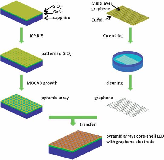
The graphene and nitride semiconductor structures were initially processed in two separate branches (Figure 1).

Figure 1: Schematic diagram of key fabrication steps for pyramid-array core-shell LED with graphene electrodes.
The nitride epitaxy began with metal-organic chemical vapor deposition (MOCVD) of silicon-doped (n-type) gallium nitride (GaN) on c-axis sapphire. This n-GaN template was then prepared for further growth with silicon dioxide used as a photolithographic mask for the growth of the pyramid structures. The 1μm holes in the mask were spaced by 1μm.
The light-emitting structures consisted of GaN pyramids grown by MOCVD for 10 minutes, multiple quantum wells (MQWs) of three-pairs of InGaN/GaN on the (1-101) semi-polar facets of the pyramids, and a 200nm layer of p-GaN. The final pyramid structures were 1.5μm in diameter and 1.5μm high. The pyramids had six (1-101) facets. It has been found that such structures filter out dislocations from threading up from the template. Growing the MQWs on the semi-polar facets, the polarization field effects are reduced. These effects can reduce LED efficiency.
Multi-layer graphene was prepared on copper foil by chemical vapor deposition using methane precursor. The graphene was spin-coated with poly(methyl methacrylate) (PMMA) and the copper removed by an iron chloride (FeCl3) solution wet etch. The graphene was then transferred to the nitride semiconductor structure and the PMMA removed in acetone. The graphene transfer process was carried out three times to improve the coverage of the pyramids. Separate measurements on graphene on glass indicated that the transmittance of such multi-layer graphene was around 95% in the visible range.
The LEDs were fabricated using a mesa etch, and the application of chromium-platinum-gold contacts. The LED chips measured 177μm x 228μm. In the process, graphene was removed selectively using photolithography and oxidation.
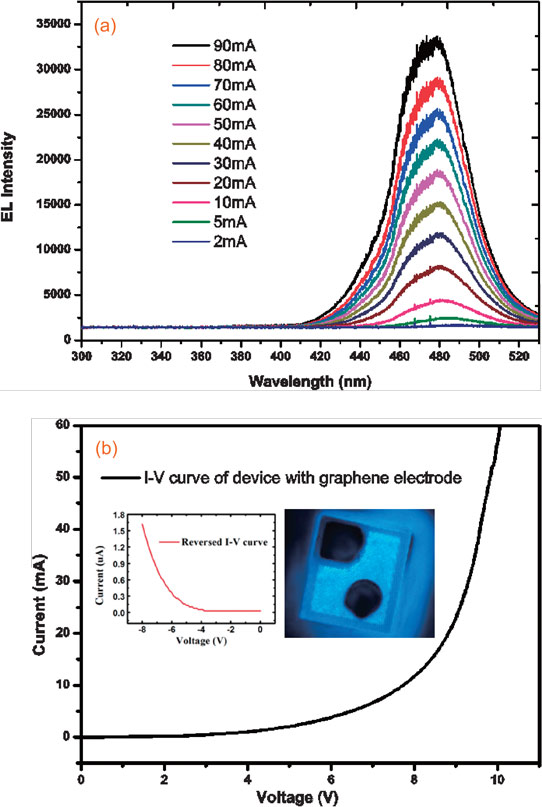
The electroluminescence of the devices peaked around 478nm “with no noticeable spectral shift as the injection current is increased from 2 to 90mA” (Figure 2). This is in contrast to conventional LEDs built from polar c-plane (0001) nitride semiconductors where the strain-dependent (piezoelectric) and spontaneous polarization fields cause a QCSE shift in the peak wavelength. The researchers believe that their pyramid LEDs structures have very small strain values and that growth on the semi-polar facets also reduces the QCSE.

Figure 2: (a) Room-temperature electroluminescence spectra of pyramid-array core-shell LEDs at various current injections. (b) Current versus voltage (I-V) curve of LEDs with multi-layer graphene electrode. Inset: photograph of light emission from single LED chip and reverse-biased current-voltage curve.
The width of the emission lines is quite broad, attributed to fluctuation in the indium composition of the MQWs. The current versus voltage behavior shows a reverse current of 1.6μA at -8V. The researchers believe this indicates that such devices would demonstrate good reliability.


