Researchers in Taiwan and USA have developed lateral insulated-gate bipolar junction transistors (IGBTs) using 4H silicon carbide (SiC) technology [Kuan-Wei Chu et al, IEEE Electron Device Letters, published online 9 January 2013]. “To the best of the authors’ knowledge, lateral n-channel IGBTs in 4H-SiC are reported for the first time,” they write.
The team consisted of researchers from Taiwan National Tsing Hua University, US Washington State University, and Taiwan’s Industrial Technology Research Institute (ITRI).
The lateral IGBTs have potential for high-voltage, high-power and high-temperature applications. Silicon carbide has a wide bandgap that allows for higher critical fields and higher temperature endurance. Often high-power/voltage performance is achieved by using ‘vertical’ current flow. However, low-voltage devices are generally based on lateral current flow. Developing lateral IGBTs creates the opportunity to monolithically integrate high- and low-voltage devices.
The transistors were created from a 2μm p-type epitaxial layer of SiC on a high-purity semi-insulating (HPSI) silicon-face 4H-SiC substrate (Figure 1). The doping for the various regions of the device were achieved using ion implantation of nitrogen (n-drift and n-buffer), phosphorous (n-emitter) and aluminium (p-collector and p-emitter).

Figure 1: Device structure of lateral IGBT in 4H-SiC. An n-type buffer is included underneath a p-collector and p-base to prevent punch-through.
Transistor formation began with mesa isolation. An optional two-step carrier lifetime enhancement process was applied to two of the device variants, consisting of two thermal oxidation steps at 1150°C for 1 hour. The aim was to reduce concentrations of two deep levels that capture carriers, reducing the lifetime.
The devices were then capped with graphite and annealed in argon at 1700°C for 10 minutes. An RCA clean process prepared the deposition of 700\Angstrom gate oxide. Next, another anneal step at 1350°C in nitrous oxide (N2O) was performed. The n+-contact consisted of titanium/nickel and the p+-contact was titanium/aluminium/nickel, which were vacuum sintered with a 3 minute rapid thermal anneal at 1150°C. The transistor was completed with a titanium/aluminium gate. A titanium/aluminium combination was also used to make metal pads for probe testing.
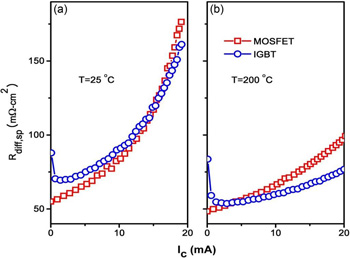
The best device (IGBT1) had a relatively light doping of the buffer with a nitrogen concentration of 3x10¹³/cm2 and used the two-step lifetime enhancement process. Such an IGBT with 20μm drift region length demonstrated a lower differential on-resistance at 30V gate potential (Figure 2) than a test SiC MOSFET at high current and high temperature (200°C). The cross-over point for room temperature was 15mA collector current. This reduced to 3.7mA at 200°C.

Figure 2: Differential specific on-resistance of MOSFET and IGBT1 (gate potential of 30V) at (a) room temperature and (b) 200°C.
The differential specific on-resistance at 20mA collector current was 161mΩ-cm2 at room temperature and 77mΩ-cm2 and 200°C.
IGBT1 with a 20μm drift region also showed increased common base current gain of the parasitic p-n-p bipolar junction transistor that is a feature of such devices. One effect of the increased gain is to increase the saturation current.
However, longer drift regions are needed to create IGBTs with higher breakdown voltage (BV) at zero gate potential. The BVs were tested while immersed in Fluorinert coolant liquid. With a 20μm drift region, the BV was 930V. Increasing the drift region to 40μm and 80μm increased the BV to 1440V and 2670V, respectively.


