Is it time for high-brightness LED manufacturing to get serious about process control? If so, what lessons can be learned from traditional, silicon-based integrated circuit manufacturing?
The answer to the first question can be approached in a straight-forward manner: by weighing the benefits of process control against the costs of the necessary equipment and labor. Contributing to the benefits of process control would be better yield and reliability, shorter manufacturing cycle time, and faster time to market for new products. If together these translate into better profitability once the costs of process control are taken into account, then increased focus on process control makes sense.
Let’s consider defectivity in the LED substrate and epi layer as a starting point for discussion. Most advanced LED devices are built on sapphire (Al2O3) substrates. Onto the polished upper surface of the sapphire substrate an epitaxial (“epi”) layer of gallium nitride (GaN) is grown using metal-organic chemical vapor deposition (MOCVD).
Epitaxy is a technique that involves growing a thin crystalline film of one material on top of another crystalline material, such that the crystal lattices match—at least approximately. If the epitaxial film has a different lattice constant from that of the underlying material, the mismatch will result in stress in the thin film. GaN and sapphire have a huge lattice mismatch (13.8%), and as a result, the GaN “epi layer” is a highly stressed film. Epitaxial film stress can increase electron/hole mobility, which can lead to higher performance in the device. On the other hand, a film under stress tends to have a large number of defects.
Common defects found after deposition of the epi layer include micro-pits, micro-cracks, hexagonal bumps, crescents, circles, showerhead droplets and localized surface roughness. Pits often appear during the MOCVD process, correlated with the temperature gradients that result as the wafer bows from center to edge. Large pits can short the p-n junction, causing device failure. Submicron pits are even more insidious, allowing the device to pass electrical test initially but resulting in a reliability issue after device burn-in. Reliability issues, which tend to show up in the field, are more costly than yield issues, which are typically captured during in-house testing. Micro-cracks from film stress represent another type of defect that can lead to a costly field failure.
Typically, high-end LED manufacturers inspect the substrates post-epi, taking note of any defects greater than about 0.5mm in size. A virtual die grid is superimposed onto the wafer, and any virtual die containing significant defects will be blocked out. These die are not expected to yield if they contain pits, and are at high risk for reliability issues if they contain cracks. In many cases nearly all edge die are scrapped. Especially with high-end LEDs intended for automotive or solid-state lighting applications, defects cannot be tolerated: reliability for these devices must be very high.
Not all defects found at the post-epi inspection originate in the MOCVD process, however. Sometimes the fault lies with the sapphire substrate. If an LED manufacturer wants to improve yield or reliability, it’s important to know the source of the problem.
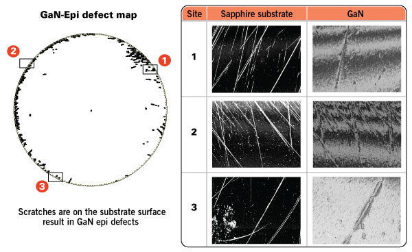
The sapphire substrate itself may contain a host of defect types, including crystalline pits that originate in the sapphire boule and are exposed during slicing and polishing; scratches created during the surface polish; residues from polishing slurries or cleaning processes; and particles, which may or may not be removable by cleaning. When these defects are present on the substrate, they may be decorated or augmented during GaN epitaxy, resulting in defects in the epi layer that ultimately affect device yield or reliability (see figure).

Patterned Sapphire Substrates (PSS), specialized substrates designed to increase light extraction and efficiency in high-brightness LED devices, feature a periodic array of bumps, patterned before epi using standard lithography and etch processes. While the PSS approach may reduce dislocation defects, missing bumps or bridges between bumps can translate into hexes and crescent defects after the GaN layer is deposited. These defects generally are yield-killers.
In order to increase yield and reliability, LED manufacturers need to carefully specify the maximum defectivity of the substrate by type and size—assuming the substrates can be manufactured to those specifications without making their selling price so high that it negates the benefit of increased yield. LED manufacturers may also benefit from routine incoming quality control (IQC) defect measurements to ensure substrates meet the specifications—by defect type and size.
Substrate defectivity should be particularly thoroughly scrutinized during substrate size transitions, such as the current transition from four-inch to six-inch LED substrates. Historically, even in the silicon world, larger substrates are plagued initially by increased crystalline defects, as substrate manufacturers work out the mechanical, thermal and other process challenges associated with the larger, heavier boule.
A further consideration for effective defect control during LED substrate and epi-layer manufacturing is defect classification. Merely knowing the number of defects is not as helpful for fixing the issue as knowing whether the defect is a pit or particle. (Scratches, cracks and residues are more easily identified by their spatial signature on the substrate.) Leading-edge defect inspection systems such as KLA-Tencor’s Candela products are designed to include multiple angles of incidence (normal, oblique) and multiple detection channels (specular, “topography,” phase) to help automatically bin the defects into types. For further information on the inspection systems themselves, please consult the second author.
Rebecca Howland, Ph.D., is a senior director in the corporate group, and Tom Pierson is a senior product marketing manager in the Candela division at KLA-Tencor.
Previous Process Watch articles include “The Dangerous Disappearing Defect,” “Skewing the Defect Pareto,” “Bigger and Better Wafers,” “Taming the Overlay Beast,” “A Clean, Well-Lighted Reticle,” “Breaking Parametric Correlation,” and “Cycle Time’s Paradoxical Relationship to Yield.”


