Researchers in Germany are proposing scandium nitride (ScN) as a suitable buffer for gallium nitride (GaN) on silicon (Si) growth [L. Lupina et al, Appl. Phys. Lett., vol107, p201907, 2015]. The attraction of ScN is a very small mismatch with GaN of less than 0.1%. This compares with the GaN/Si mismatch of ~17%.
However, when ScN is grown directly on silicon the resulting material suffers from serious crystal defects. The team – from IHP, Technische Universitt Berlin, SILTRONIC AG, and BTU Cottbus – has developed a growth technique where yttrium (Y2O3) and scandium (Sc2O3) oxide are grown first. These layers allow single-crystal layers of ScN to be developed that avoid stacking faults away from the interface. The mismatch between ScN and Sc2O3 is estimated at 8.5%.
The researchers see potential application for GaN devices such as light-emitting diodes, laser diodes, photo-detectors, and high-power and high-frequency electronics.
The researchers comment that "based on the use of highly insulating oxides, the ScN/Sc2O3/Y2O3/Si buffer approach can, in principle, be further engineered for improved electrical breakdown field strength with respect to the Si interface, which is of importance for high-power/high-frequency applications of GaN-on-Si systems."
The researchers prepared templates with Sc2O3 and Y2O3 layers on 4-inch (111) silicon (Sc2O3/Y2O3/Si) by molecular beam epitaxy. The scandium nitride was grown on the template in a plasma-assisted molecular beam epitaxy (PAMBE) reactor chamber with electron-beam evaporation of elemental scandium and nitrogen radio-frequency plasma as sources.

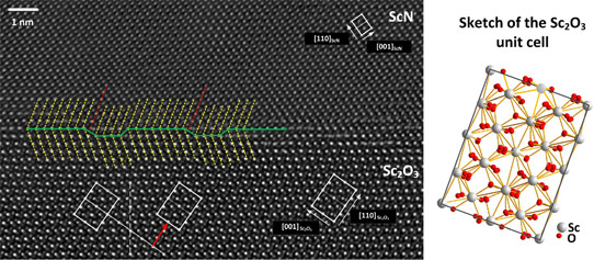
Figure 1: High-resolution transmission electron microscope (HRTEM) image obtained on Sc2O3 (lower part)/ScN (upper part) interface and sketch of Sc2O3 unit cell. The red vector indicates stacking fault in anion sublattice of Sc2O3.
X-ray and electron microscope analysis showed that the overgrown ScN layer was a single crystal with 'rock salt' structure (Figure 1) for growth temperatures less than 700°C. Additional x-ray diffraction peaks appear above 700°C that indicate that the material then consisted of differently oriented ScN crystal grains, along with polycrystalline regions. These defects are thought to arise due to decomposition of the oxide buffer or the formation of Sc2O3/ScNO during the ScN growth.
The tensile strain was also assessed using x-ray analysis. It was found to increase with temperature. The researchers attribute this to strong oxygen incorporation in the ScN at higher temperature. They report: "This hypothesis was verified by a comprehensive investigation of the ScN/Sc2O3 interface using x-ray photoelectron spectroscopy, time-of-flight secondary-ion mass spectrometry, transmission electron microscope-energy dispersive x-ray spectroscopy, and ab-initio calculations, which will be reported in a separate publication."
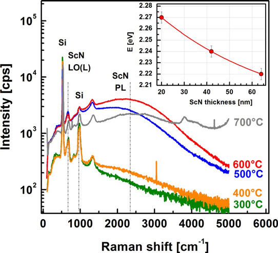
Raman analysis of phonon/lattice vibration effects on photoluminescence suggested that material grown at 300°C and 400°C suffered from lower optical quality, probably due to point defects (Figure 2). The researchers concluded that 600°C was an optimal growth temperature.

Figure 2: Room-temperature Raman spectra of about 20nm-thick ScN layers deposited at temperatures ranging from 300°C to 700°C. Excitation wavelength of 488nm was used as pump source. Inset: ScN bandgap obtained from ScN photoluminescence peak plotted as a function of ScN film thickness, grown at 600°C.
The ScN energy bandgap was found to decrease with the thickness of the layer. The researchers suggest that this is due to decreasing oxygen concentration in thicker layers. The bandgap of Sc2O3 is 6.0eV and that of bulk ScN is 2.1eV. Bandgaps for ScON compounds would be expected to be between these values.
The researchers report: "For an about 60nm-thick ScN layer, a bandgap value of about 2.22±0.005eV is extracted, indicating a relatively low oxygen level in the main part of the film."
The 600°C material also was found in further x-ray analysis to be free of stacking twin defects, where the layer sequence changes to another type and back again to the original. The researchers comment: "It is noted that this result is in contrast to the observations done for ScN films grown directly on Si(111) substrates."


