The Group of III-V Semiconductors of the Solar Energy Institute at the Technical University of Madrid (Instituto de Energía Solar at Universidad Politécnica de Madrid, IES-UPM) has developed a highly conductive, high-bandgap p++-AlGaAs/n++-GaInP tunnel junction (TJ) grown by metal-organic vapour phase epitaxy (MOVPE) with what is reckoned to be outstanding electrical performance, for application in ultra-high-concentration multi-junction solar cells. The TJ is intended to interconnect the top (GaInP) and middle (GaInAs) subcells of triple-junction concentrator photovoltaic (CPV) cells. In as-grown tunnel diodes, an average peak tunneling current density (Jp) of 996A/cm2 and a specific resistance of 7x10⁻⁵Ωcm2 were obtained, whilst record-performing devices exhibited Jp above 1050A/cm2.

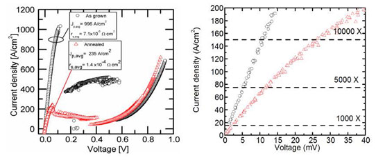
Left: Average J-V measurements of p++-AlGaAs:C/n++-GaInP:Te TJs fabricated with the as-grown structures (black circles) and after thermal annealing at 675oC for 30 min (red triangles). Right: Magnification of left figure for low voltages where current densities equivalent to operation at 1000, 5000 and 10000 suns are drawn as references (dotted lines).
However, it is well documented that, when introduced in multi-junction solar cell structures, tunnel diodes suffer significant degradation as a result of the thermal load associated with the growth of the rest of the solar cell structure, which typically occurs at much higher temperatures as those used for the growth of the tunnel diode. In order to simulate this effect, researchers at IES-UPM annealed the samples which, after the thermal load, still exhibited high performance, with average Jp reduced to 235A/cm2 and specific resistance raised to 1x10⁻⁴Ωcm2 . Despite this drop, these values are still high enough by far to allow the TJ to operate in the ohmic region up to about 15,000 suns with negligible voltage drop (see Figure).
The design and manufacture of multi-junction solar cells - and accordingly tunnel junctions - for operation at ultra-high concentration (i.e. several thousand suns) is one of the research goals of the III-V Semiconductor Group at IES-UPM. In 2008, a GaInP/GaAs dual-junction solar cell with a record efficiency of 32.6% at 1026 suns was achieved [‘A 32.6% efficient lattice-matched dual-junction solar cell working at 1000 suns’, Garcia et al, Appl.Phys. Lett. 94 (2009) 053509]. The TJ employed in that case (a p++-AlGaAs:C/n++-GaAs:Te) showed peak current densities of 2000 and 300A/cm2 for the as-grown and annealed devices, respectively. (See also ‘Performance analysis of AlGaAs/GaAs tunnel junctions for ultra-high concentration photovoltaics’, I García et al, J. Phys. D: Appl. Phys., 45 (2012) 045101.)
With the aim of improving the transparency of that TJ design, the new TJ has been developed by substituting the GaAs-based cathode by a GaInP alloy. In fact, the optical improvement results in a gain in current of about 0.56A/cm2, which implies an improvement of 1.3% (absolute) in triple-junction solar cell efficiency – see ‘Highly conductive p++ -AlGaAs/n++ -GaInP tunnel junctions for ultra-high concentrator solar cells’, Barrigón et al, Progress Photovoltaics 22 (2014), p399.
Researchers at UPM believe that all these characteristics could make this TJ structure a key element in their quest to develop high-efficiency solar cells for operation at ultra-high concentrations.


