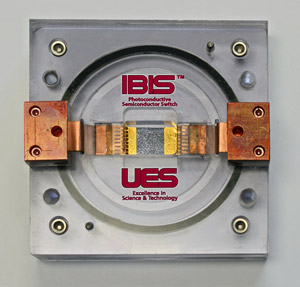
Science & technology research firm UES Inc of Dayton, OH, USA says that its IBIS photoconductive semiconductor switch (PCSS) has been selected by an independent judging panel and the editors of R&D Magazine as a winner of a 2015 R&D 100 Award in the IT/Electrical category. An R&D 100 Award recognizes the 100 most technologically significant products introduced in the past year.

Picture: UES' IBIS photoconductive semiconductor switch.
Advanced pulsed power switching technologies such as IBIS PCSS enable future nuclear weapon effects (NWE) experimentation capabilities and concepts for the active interrogation of special nuclear materials (SNM). The gallium arsenide (GaAs)-based IBIS PCSS device handles up to 75kV operating voltage, with a total current of ~1kA. Individual channel current has been measured at around 20A/channel at 1kA, with a rise time of 600-800ps. The device has functional dimensions of just 1-2cm per side, and can be triggered with low incident energies of 50-150 microjoules/cm2. UES says that the specifications of the patent-pending technology significantly extend the operation windows of currently available PCSS technology, maintaining stringent CSWAP constraints.
UES says that it achieved the honor by:
proposing to and winning consecutive Small Business Innovative Research (SBIR) and Rapid Innovation Fund (RIF) awards from the Defense Threat Reduction Agency (DTRA); and converting the technology developed in the SBIR process to an electromagnetic pulse generator for nuclear pulse simulation, in partnership with L3 Inc.
"I'm grateful for the consistent partnerships and support from Hoa Nguyen of DTRA, and Doug Weidenheimer at L3," notes the device's inventor Dr Rabi Bhattacharya.
"This recognition highlight UES' core strengths of developing and incubating an innovative technology, and working well with key stakeholders to bring it to reality," says CEO Dr Nina Joshi.


