Researchers in Singapore claim the first DC and microwave performance measurements for 0.15μm-gate aluminium gallium nitride(AlGaN)on gallium nitride high-electron-mobility transistors(HEMTs)on silicon substrates with gold-free metallization[Subramaniam Arulkumaran et al,Appl.Phys.Express,vol6,p016501,2013].
The development of gold-free source,drain,gate and interconnects is important for the easy transfer of GaN-based devices onto an integrated complementary metal-oxide-semiconductor(CMOS)transistor platform.Gold contamination poisons silicon semiconductor performance.Gold-free processing is also relevant where manufacturers may want to run separate GaN transistor fabrication wafers alongside traditional silicon device wafers.
The research is therefore of interest in developing GaN device production on large-diameter silicon(up to 12-inch diameter versus~2-4-inch on sapphire and silicon carbide)for economies of scale.GaN devices can achieve high-frequency performance(up to 370GHz cut-off)and large power density(~2.5W/mm at 40GHz)due to the wide bandgap and high critical electric field for breakdown.
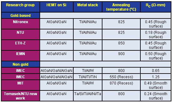
Researchers based at Temasek Laboratories and Nanyang Technological University(NTU)in Singapore developed the gold-free process with low contact resistance(Table 1).In fact,the Temasek facility is also sited at the Nanyang campus.

Table 1:Contact resistance values for different GaN HEMT structures on Si substrate using conventional III–V gold-and CMOS-compatible non-gold-based ohmic stacks.
The heterostructure for the HEMT consisted of a 4-inch high-resistivity silicon substrate(resistivity greater than 6000Ω-cm),1.4μm GaN transition layer,800nm GaN buffer,18nm Al0.26Ga0.74N barrier,and 2nm GaN cap.The researchers used metal-organic chemical vapor deposition(MOCVD)as the nitride semiconductor heterostructure growth process.The resulting electron transport properties were 1450cm2/V-second mobility and 1.1x10¹³/cm2 sheet carrier density.
The transistors were fabricated using mesa isolation,ohmic metal deposition and gate fabrication.The ohmic metal stack was tantalum/silicon/titanium/aluminium/nickel/tantalum.After annealing in nitrogen at 800°C for 30 seconds,the typical contact resistance was 0.24Ω-mm(standard deviation 0.07Ω-mm).Three separate runs of the ohmic metal process were performed.The average specific contact resistivity was 1.5x10⁻⁶Ω-cm2.
The researchers comment:"The achieved contact resistance is believed to be the lowest ever reported for non-gold ohmic contacts for conventional AlGaN/GaN HEMTs on Si and it is also lower than that of recessed ohmic contacts."(See Table 1.)
Recessing is used to reduce contact resistance,but tends to increase process complexity and hence production costs.
The T-gate formation process consisted of a 30 minute ammonium sulfide pre-treatment,120nm silicon nitride plasma-enhanced chemical vapor deposition(PECVD),0.15μm-gate footprint opening by patterned etch,and nickel/aluminium/tantalum(100/400/30nm)gate head formation.The gate dimensions were:source–gate distance of 0.8μm,gate–length of 0.15μm and gate–drain distance of 1.7μm.The width of the gate was 2x75μm.
The fabrication was completed with a titanium/aluminium/tantalum(50/800/30nm)interconnect metal stack and final passivation with a further 120nm of silicon nitride.
The metals chosen for use"are commonly used in the silicon fabrication process line and,hence,they will not introduce any cross-contamination in the manufacturing lines."
The maximum drain current was 830mA/mm and the peak extrinsic transconductance was 250mS/mm.The threshold voltage was negative(depletion-mode,normally-on)at-3.75V.The reverse-biased gate leakage current was 3.8x10⁻³mA/mm at-20V.
The small-signal gain frequency performance was measured between 6GHz and 40GHz.The cut-off frequency(fT)was 39GHz and the maximum oscillation(fmax)was also 39GHz.The researchers believe this to be"the first reported microwave performance of submicron AlGaN/GaN HEMTs using CMOS-compatible non-gold metal stacks".
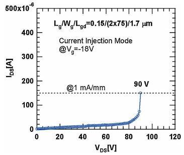
Current collapse with pulsed currents was less than 10%.The three-terminal OFF-state breakdown voltage(BVgd)was 90V(Figure 1).The Johnson figure of merit of fT x BVgd was 3.51-3.83THz-V for gate-drain spacings in the range 1.7-3.5μm.

Figure 1:Three-terminal OFF-state breakdown voltage characteristics of HEMT with CMOS-compatible non-gold metal stack and 1.7μm gate–drain spacing.
The researchers comment:"The obtained values are comparable to that of the 0.15μm gate-length GaN HEMTs(3.3THz-V)on Si(111)fabricated using a conventional III–V gold-based metal stack."
The team concludes:"These results demonstrate the feasibility of non-gold metallization process to achieve submicron-gate AlGaN/GaN HEMTs on Si substrate for high-frequency applications."


