Asahi Kasei Microdevices Corporation and Kyushu University in Japan detectors based on indium antimonide (InSb) [Koichiro Ueno et al, Jpn. J. Appl. Phys., vol52, p092202, 2013].
The reshave developed room-temperature mid-infrared semiconductorearchers believe such devices could be used to save power in facilities where no people are present through the detection or not of human body heat.
The human body gives out detectable thermal radiation in the range 3-25μm, peaking around 10μm (essentially a Planck blackbody distribution for 36-37°C). The Asahi Kasei/Kyushu device covers the 2-7μm range.
Present methods of detecting humans tend to depend on measuring temperature changes (e.g. pyroelectric devices), so if the people are stationary a false signal to turn off power could be sent. However, mid-infrared semiconductor detectors usually need cooling to operate.
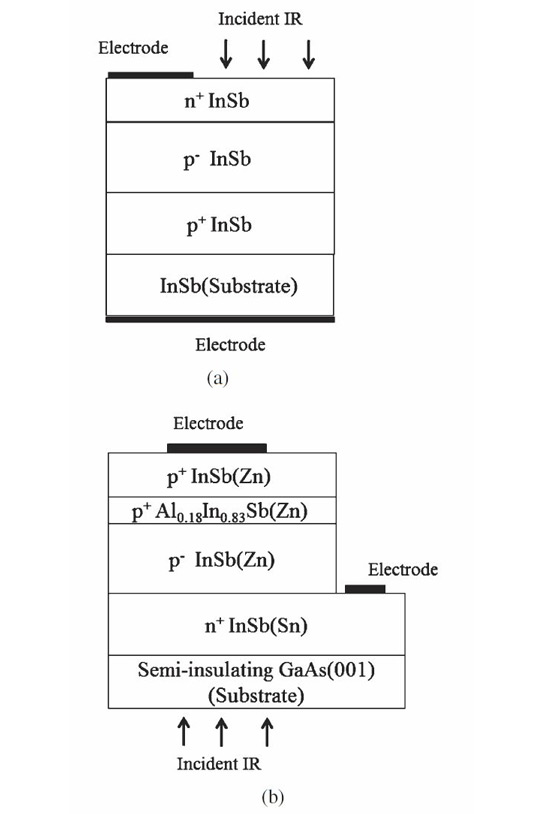
To enable room-temperature operation, the researchers worked to reduce the non radiation part of the current ('the diffusion current') of the device by increasing the resistance under zero bias (R0). The device also featured improved IR incidence efficiency by gathering radiation through the gallium arsenide (GaAs) substrate rather than through InSb layers. In addition, the GaAs surface was roughened to reduce reflection.

Figure 1: (a) Conventional InSb infrared sensor structure and (b) Asahi Kasei/Kyushu sensor structure.
The indium antimonide (InSb) photodiode structure (Figure 1b) was grown on a semi-insulating (001) GaAs substrate using Riber MBE-49 molecular beam epitaxy system. The substrate temperature during growth was 410°C. The group V (Sb) to group III (In) flux ratio was 2:1. Tin (Sn) and zinc (Zn) were used to dope InSb with n- (electrons) and p-type (holes) carriers. The Zn doping was carried out at high concentration due to the element's high volatility with low sticking coefficient in InSb.
The material was fabricated into photodiodes using photolithography and chemical etch. The electrodes consisted of aluminium/titanium.
The researchers optimized the n-type doping so that more than 80% of IR light with wavelengths longer than 3μm could penetrate the n-InSb layer. The point at which this occurred was 4.3x10¹⁸/cm3 doping concentration. At lower concentrations, the 80% value was achieved at longer wavelengths, cutting off at near 7μm with around 2x10¹⁶/cm3 doping. Although the absorption band edge did not shift much after 6x10¹⁸/cm3, the researchers decided to use 7x10¹⁸/cm3.
Another aspect that needed optimization was the heavily p-type aluminium indium antimonide (p+-AlInSb) barrier. The resistance under zero bias (R0) was maximized with an Al-fraction of 18%. Also the barrier was set at 20nm, since thicker AlInSb layers showed reduced R0. X-ray analysis suggested that this was due to degradation of crystallinity from lattice mismatch causing generation of defects. The defects in the AlInSb also caused degradation of the p-InSb layer above the barrier.

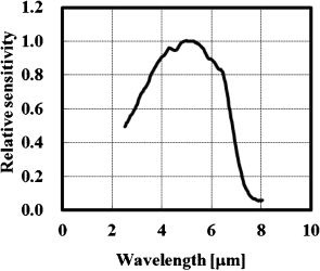
Figure 2: InSb photodiode relative spectral sensitivity characteristic.
The effect of the optimized barrier is to reduce carrier leakage, as reflected by a 70% increase in R0 over photodiodes without barrier.
The GaAs substrate was also mechanically thinned in a process that also produced surface roughening to reduce reflection of the incoming IR. An increase of photocurrent of around 25% was achieved by roughening. For the complete device, an average absolute value (Ra) roughening around 200nm was chosen.
The resulting device was sensitive in the wavelength range 2-7μm. The junction area was 210μm2.
To increase the open circuit voltage and R0 value of the detector, 700 photodiodes were patterned on a 600x600μm chip and connected in series. The effective junction area of each diode was 100μm2. The chip was encapsulated in a non-leaded quad flat pack with the roughened GaAs substrate uppermost in a window in the top of the package. The detector dimensions were 2.2x2.7x0.7mm.
The packaged detector chip demonstrated a typical responsivity of 1900V/W, output noise of 0.15μV/Hz1/2 at 300K, and detectivity of 2.8x10⁸Hz1/2/W at 300K. The researchers conclude: "This performance is high enough for our device to be used as an uncooled mid-infrared photon detector."


