Demonstration of functional components brings Si photonics closer to CMOS standards.
imec results announced at Semicon West
Imec has successfully demonstrated the creation of functional sub-100 nm photonics components on 300 mm silicon wafers with optical lithography,in what the organization believes is a world first.
Announced at Semicon West in San Francisco,the news could represent an important step towards bringing silicon photonics technology into line with CMOS industry standards.
The breakthrough comes out of imec's industrial affiliation program on optical I/O,in which the Belgian research hub is working with a number of key players is the development of Si photonics processes,devices and circuits,using state-of-the-art CMOS fabrication processes.
Many nanophotonics components have previously only been demonstrated using lab-scale techniques such as e-beam lithography,but imec's announcement relates to the successful demonstration of functional devices on industry-compatible 300 mm wafers using 193 nm immersion lithography and 28 nm CMOS processes.This could represent a route for Si photonics to move closer to adoption by the wider CMOS sector.
"It's definitely great to see these photonics processes being moved up to 300 mm,"commented Michael Hochberg,a founder of Luxtera who now heads the OpSIS wafer center."This will be important as silicon photonics starts to be used for very high volume applications.The data they are generating is going to be very valuable to the community in understanding the trade-offs between mask cost,wafer cost,volume production costs,and photonic device performance."
Imec itself is equally bullish about the significance of the demonstration."Possible applications include next-generation short-reach interconnects,which we expect to go into manufacturing by 2015,"said Philippe Absil,director of the optical I/O program at imec.
Fabless ecosystem
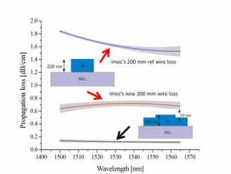
The silicon waveguides announced at Semicon West showed propagation losses well below 1 dB/cm.Imec believes that by applying 193?nm immersion lithography for patterning waveguides as well as fiber couplers,it has successfully eliminated one patterning step in the processing of photonics devices,which could result in a significant cost reduction as the process becomes commercialized.
Such adoption could follow readily,according to silicon photonics advocates.Hochberg recently told optics.org he believes that the age of the silicon photonics economy is already well underway.
"There are at least a dozen big semiconductor companies or well-funded start-ups that I'm aware of who are now making and selling silicon photonics components,or who are on the path to doing just that,"he said."You can also see this development in recruitment of PhDs;people who can integrate and design these things are incredibly in demand at the moment."
OpSIS is intended to play its part by opening up Luxtera's silicon CMOS photonics device library and processes to the OpSIS community,thanks to an agreement between the two organizations.It also aims to make the manufacturing processes for optoelectronic integrated circuits available to the community at modest cost,by sharing some of the processing expenses across many users.Doing so will advance the field by bringing prototyping capability within reach of startups and academic research groups.
"If we,as the photonics industry,are going to be successful on the same scale as the electronics industry we must replicate the fabless ecosystem,"commented Hochberg,describing his vision."It must be possible to train an undergraduate to design photonics circuits.If you want to crystallize what our goal is as Opsis into one sentence then that's what we want to achieve."


