Researchers in Nanjing,China have reported the first fabrication and characterization at high temperature of high-performance solar-blind photodetectors(PDs)based on an aluminium gallium nitride(AlGaN)absorption layer and planar metal-semiconductor-metal(MSM)electrode layout[Feng Xie et al,IEEE Sensors Journal,vol12,p2086,June 2012].The participating institutions were Jiangsu Provincial Key Laboratory of Advanced Photonic and Electronic Materials/Nanjing University and Nanjing Electron Devices Institute.
The new devices have an ultra-low dark current in the femtoamp(fA=10-15A)range,even at 150°C.At room temperature(RT),the solar-blind/ultraviolet rejection ratio is four orders of magnitude,and even at 150°C its value is more than 8000.The researchers comment on their device:"The ultra-low dark current and the high rejection ratio at 150°C suggest that such PDs are suitable for high-temperature applications."
These potential applications include missile plume sensing,flame detection,environmental monitoring,chemical/biological agent detection,and covert space-to-space communications.
Presently,solar-blind detection is achieved using fragile photomultiplier tubes or silicon photodetectors,which need complex and expensive filters,and bulky high-voltage power supplies.Also,these devices and their support systems can be sensitive to harsh environments such as that found in gas turbines.
Aluminium gallium nitride(AlGaN)is naturally solar blind due to its large bandgap.The wide bandgap of the material also allows higher-temperature operation.Radiation hardness is another attractive feature.
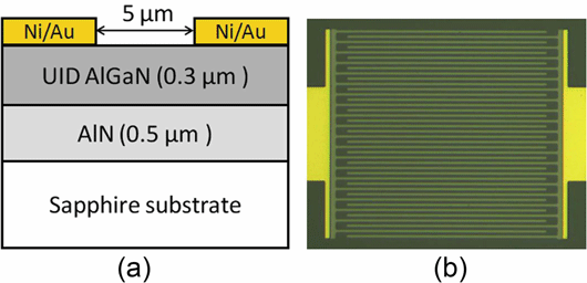
The epitaxial device structure(Figure 1)was grown on 2-inch sapphire substrate using metal-organic chemical vapor deposition(MOCVD).The 1100°C AlGaN layer was not intentionally doped.The 40%Al content of the AlGaN layer was confirmed by a 272nm cut-off in optical transmission spectroscopy.The AlN buffer was designed to be highly resistive,and was grown according to the researchers'proprietary high-temperature recipe.

Figure 1:(a)Schematic of the device structure and(b)top-view image of one fabricated PD with an effective device area of 400μm x 400μm.
The device processing began with applying thin semi-transparent layers of 5nm nickel and 5nm gold,forming a Schottky contact.Lithography and lift-off processing was used to define interdigitated electrodes that were 400μm long and 5μm wide.The electrode separation was 5μm.The nickel-gold contacts had a transmittance of 35-43%in the 200-400nm ultraviolet wavelength range.
The devices were completed by adding 200nm-thick titanium-gold contact pads and annealing at 300°C for 3 minutes in nitrogen.
The dark current at room temperature(RT)is less than 1fA(1.25x10⁻¹²A/cm2 density)and,for 150°C operation,is still in the fA range for bias voltages less than 20V.The RT breakdown occurs at more than 300V.
The very low dark current is attributed to the high Schottky barrier height of the nickel contact metal,along with the use of a high-temperature AlGaN absorption layer and the coplanar configuration of the metal-semiconductor-metal structure.Although there are still threading dislocations in the AlGaN buffer,it is thought that these terminate at the highly resistive AlN,so any lateral conductive path between the electrodes is cut off.
The photocurrent increases rapidly with biases below 2V,but then increases more slowly beyond that.At 150°C,the photocurrent is 20-40%lower than that at RT.The researchers explain this as being due to enhanced carrier recombination loss at higher temperatures.
The devices show a peak response around 275nm wavelength and a cut-off above 280nm that corresponds to the band edge of the AlGaN absorption layer(Figure 2).At 10V bias,the peak responsivity is 143mA/W,corresponding to a peak quantum efficiency of 64%.At the same bias,the solar-blind/UV rejection ratio(comparing responses at 275nm and 350nm)is as high as 1.8x10⁴ at RT and is still high(8.6x10³)at 150°C.


