Oxford Instruments is offering an upgrade option for its ALD equipment to apply a bias voltage to the substrate, adding further control of the energy at the wafer surface in order to tune the properties of the deposited film. While scaling to smaller features has been the main driver of demand for ALD to date, the developers of the coming generation of More-than-Moore products – from MEMS, to power semiconductors, to LEDs and other photonics – are increasingly looking to the process' atomic control of deposition to design optimized materials for their particular applications.
Substrate biasing has long been used with plasma-assisted CVD and PVD, but it is now starting to be explored in ALD with intriguing work by researchers at the Eindhoven University of Technology in the Netherlands. The team led by Prof.dr.ir. Erwin Kessels (W.M.M. Kessels) recently demonstrated the ability to control density, crystallinity and residual stress during the atomic layer deposition of numerous films.
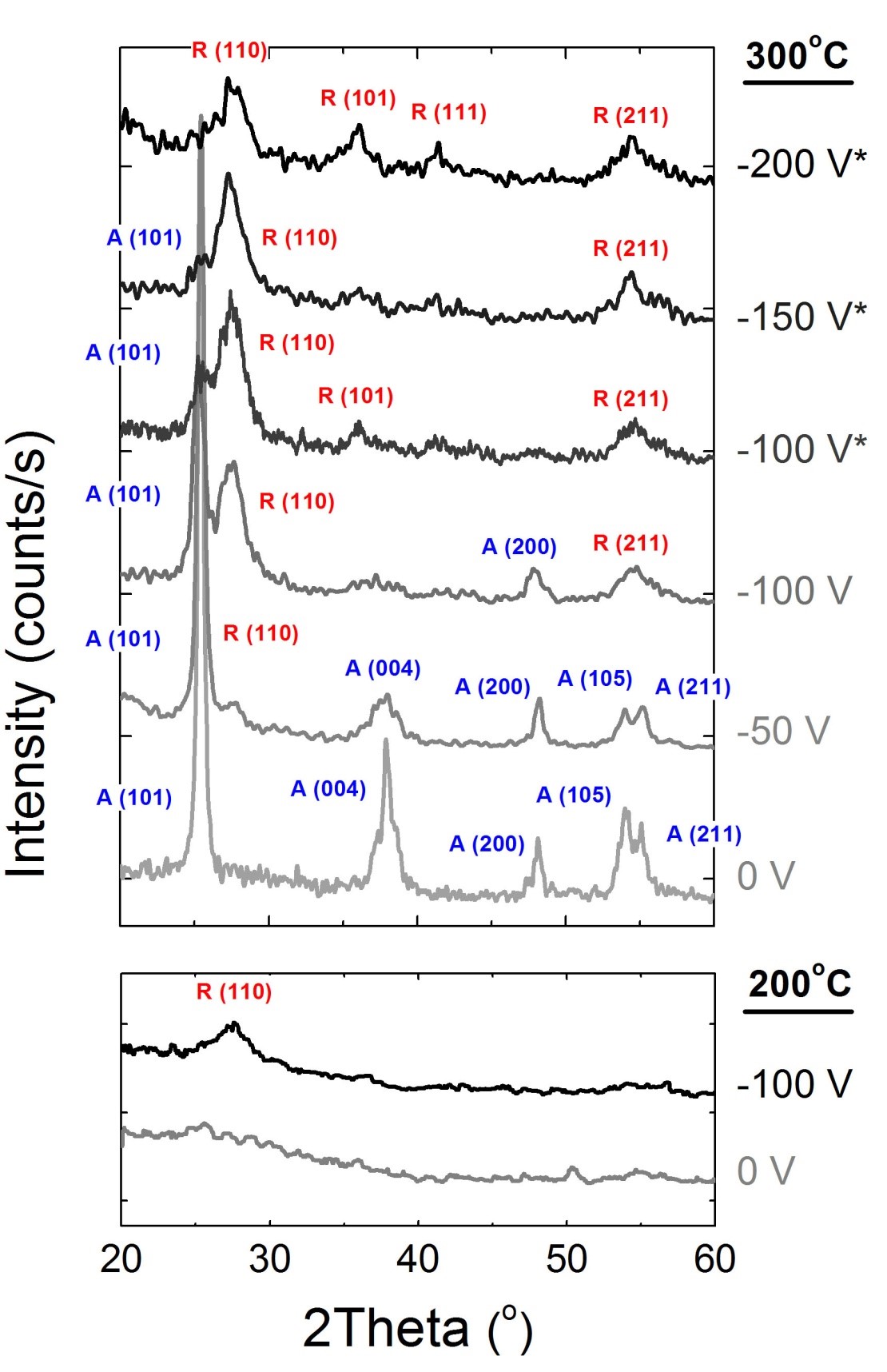
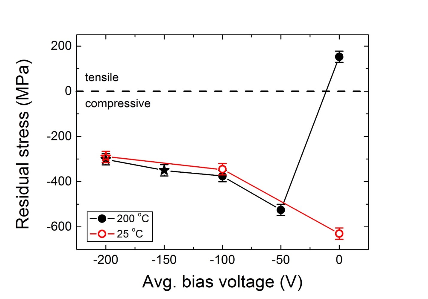
The Eindhoven research group reports1 that applying a negative average voltage of up to -200V to the substrate stage – by adding an RF power supply – increased the energy of the ions at the substrate surface up to 250eV during an O2 plasma exposure. This control of the ion energy allows precise control of material properties of the deposited film, but exactly what properties can be controlled varies from material to material. Researchers at Eindhoven have shown that applying substrate bias during atomic layer deposition of TiO2 moves the crystalline phase of the film from anatase to rutile, creating as-deposited rutile TiO2 and bringing the additional benefits of a higher dielectric constant [Figure 1]. "Through substrate biasing you can skip the post-deposition annealing step traditionally used to achieve the rutile phase and therefore lower the thermal budget of the sample," explains Annika Peter, Oxford's lead ALD technologist. Varying the ion energy during deposition of Al2O3 changes the residual stress from tensile to compressive [Figure 2] which has strong implications in MEMS devices, where the fine control of stress on free-standing structures, such as cantilevers, is integral to device performance. Higher bias voltages can also create higher density films in the case of Co3O4.
Oxford Instruments' technologists expect that control of the ion energy will enable the design of films with other optimized characteristics, or with simpler process requirements. "This is very new – a new dial to very easily tune the physical properties of specific materials," notes Robert Gunn, Plasma Technology Business Group Manager. "We now need to explore the physics behind the material interactions to see what applications this would be relevant to."
What will be the driving market? "It might be easier to ask what market it won't fit into," suggests Frazer Anderson, Nanotechnology Tools Business Group Director.

Figure 1: Change in crystal phase of TiO2 from pure anatase (A) with 0V bias to pure rutile (R) at -200V, measured using x-ray diffraction analysis1 (Profijt et al, 2012)

Figure 2: Control of residual stress in an Al2O3 film from tensile to compressive at 200 °C
More-than-Moore markets turn to ALD for optimizing material properties
A variety of semiconductor markets are looking to ALD for this control of material properties instead of scaling size. Gunn notes increasing interest from makers of power semiconductors in atomic-level layering of different materials to create unique combinations of their different properties. Combining atomic layers of hafnium oxide with layers of aluminum oxide, for example, can engineer a material with the usually mutually-exclusive characteristics of the two materials –both the high dielectric constant of the hafnia and the high breakdown voltage of the alumina. The ability to precisely control the ion energy in Oxford Instruments' PEALD equipment minimizes the plasma damage to the underlying surface, while maintaining the high film quality associated with a plasma-enhanced deposition, a big issue for power applications, says Peter.
ALD technology is also drawing interest from the MEMS sector for its potential to optimize material properties for MEMS structures. ALD offers uniform coverage of high aspect ratio features and the potential for optimizing anti-stiction or passivation coatings, but could also enable the design of materials with specific mechanical properties for particular structures. "As MEMS get smaller and more complex, ALD gets more interesting to do the things that PECVD can't do," says Gunn.
In the compound semiconductor and photonics sector, ALD provides options to deposit a wide range of materials at lower temperature, such as growing GaN on silicon from a metal organic. ALD Applications Scientist Thomas Sharp has demonstrated GaN growth on silicon, as well as silica and titanium nitride, down to 150°C and notes that work is ongoing to improve the degree of crystallinity.
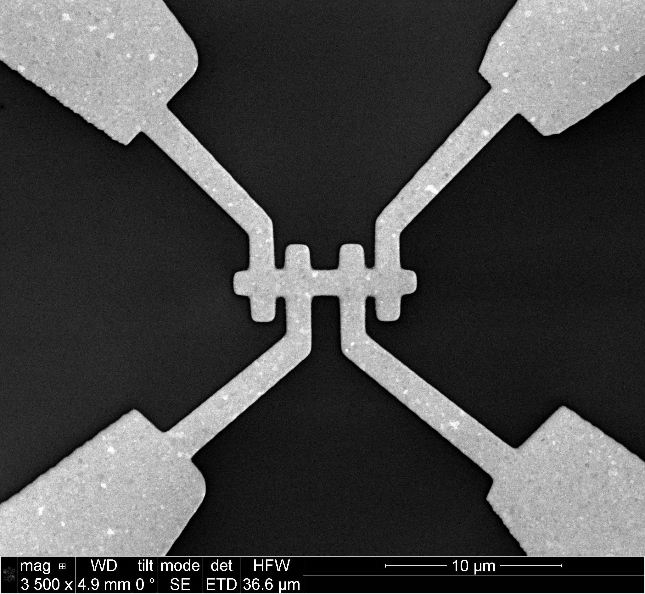
Demand for ALD is also coming from researchers working on the deposition of the 2D and 1D nanomaterials under consideration for future IC applications, such as graphene, carbon nanotubes and nanowires. Anderson says it's a likely option for growing the single-atomic-layer 2D materials like molybdenum disulfide and boron nitride that likely will be layered with graphene to make electronic devices. ALD also looks to be a strong candidate for the creation of contacts with 1D structures such as carbon nanotubes and nanowires, problematic interfaces where high resistance typically hinders the transfer of electrons between these structures and the larger 3D surrounding features. Researchers from Eindhoven have demonstrated ALD platinum contacts on CNT transistors made by a thin e-beam seeding film and a tuned platinum ALD process to exploit the long nucleation delay on some surfaces and promote selective growth.2

Figure 3: SEM image of four-point-probe structure formed by initial EBID patterning, and subsequent purification and thickening by an area-selective ALD Pt process
The first technology business to be spun out from Oxford University over fifty years ago, Oxford Instruments is now a global company with over 1900 staff worldwide and is listed on the FTSE250 index of the London Stock Exchange (OXIG). Its objective is to be the leading provider of new generation tools and systems for the research and industrial sectors.
Its plasma technology group offers flexible, configurable process tools and leading-edge processes for the precise, controllable and repeatable engineering of micro- and nano-structures. Products range from compact stand-alone systems for R&D, through batch tools and up to clustered cassette-to-cassette platforms for high-throughput production processing. Long-standing research partnerships with world class institutions which include Eindhoven University of Technology, Lawrence Berkeley National Laboratory in California, ITRI in Taiwan, and the Universities of Southampton and Glasgow in the UK promise further exciting research in the coming years.
1 H. B. Profijt, ∗ M. C. M. van de Sanden, and W. M. M. Kessels; Substrate Biasing during Plasma-Assisted ALD for Crystalline Phase-Control of TiO2 Thin Films; Electrochemical and Solid-State Letters, 15 (2) G1-G3 (2012)
2 Mackus, A.J.M, Dielissen, S. A. F., Mulders J. J. L., and Kessels W. M. M.; Nanopatterning by direct-write atomic layer deposition, Nanoscale, 2012, 4, 4477


