Optical waveguide connects semiconductor chips 04 Oct 2012 Technique suits high-performance emitter-receiver systems for optical data transmission.

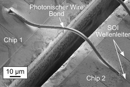
KITted out:The novel optical wire bond is adapted to the position and orientation of the chips.A team of researchers at Karlsruhe Institute of Technology(KIT)has developed a novel optical connection between semiconductor chips. Photonic wire bonding can achieve data transmission rates in the range of several terabits per second and team leader rofessor Christian Koos says the technique is"suited perfectly for production on the industrial scale".
"In the future,this technology may be used in high-performance emitter-receiver systems for optical data transmission and,thus,contribute to reducing energy consumption of the internet,"he added.The team of scientists led by Koos have published their results in the journal Optics Express(Vol.20,No.16;30 July 2012).
Communication processes can be made more quickly and more energy-efficient with photonic components.The development of high-performance optical emitters and receivers integrated on microchips has already reached a high level.However,the KIT team says that there have not yet been any satisfactory possibilities of bridging semiconductor chips optically.
Alignment is the key
'The biggest difficulty consists in aligning the chips precisely such that the waveguides meet."explains Koos,who is professor at the KIT Institutes of Photonics and Quantum Electronics(IPQ)and of Microstructure Technology(IMT)as well as member of the Center for Functional Nanostructures(CFN).
His team has tackled the problem,as he puts it,"from the other side".The researchers first fix the chips and then structure a polymer-based optical waveguide so that it fits perfectly.To adapt the interconnection to the position and orientation of the chip,the scientists developed a method for the three-dimensional structuring of an optical waveguide.They used so-called two-photon polymerization,which achieves the high resolution.
A femtosecond laser writes the free-form waveguide structure directly into a polymer that is located on the surface of the chip.For this purpose,the KIT researchers use a laser lithography system made by Nanoscribe,a spinoff company from KIT. Prototypes of the photonic wire bonds have achieved"very small losses and a very high transmission bandwidth in the range of infrared telecommunication wavelengths around the optical communications window of 1.55 micrometers".
In early experiments,the researchers demonstrated data transmission rates in excess of 5 terabits per second.Potential applications of photonic wire bonds are in complex emitter-receiver systems for optical telecommunication as well as in sensor and measurement technology Koos explained.
As the highly precise orientation of the chips in manufacturing is no longer required,the process is particularly suited for the automatic production of large series.KIT researchers now plan to transfer this technology to industrial application in cooperation with partner companies.


