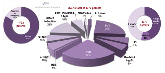
Despite a cumulative silicon carbide (SiC) raw wafer and epiwafer market that will not exceed $80m in 2012, the body of related patents comprises more than 1772 patent families and over 350 companies since 1928, according to the report ‘SiC Patent Analysis single crystal, wafer and epiwafer manufacturing’ to be published by market research firm Yole Développement at the end of July. Of total patents, 83% of patents represent a method while 17% of them claim an apparatus.
Since 1978 the main technique for growing bulk single crystals of SiC has been physical vapor transport (PVT, a seeded sublimation method), which represents 36% of published patents. The PVT technique deals mostly with the hexagonal polytype nH-SiC (n=2,4,6). An alternative route to grow SiC is liquid-phase epitaxy (LPE), for which early efforts date back to 1961. LPE allows the growth of crystals with low dislocation densities and at relatively low temperatures (attractive for cubic polytype 3C-SiC).

Figure 1: Distribution of SiC crystal, wafer and epiwafer patents by technology.
About 37% of patents involve chemical vapor deposition (CVD), which is now used almost exclusively to manufacture SiC epiwafers. In contrast, molecular beam epitaxy (MBE) is only mentioned in 1% of patents. The polytype (hexagonal or cubic) is explicitly claimed in 15% of patents. Numerous strategies to reduce crystal defects (micropipes, carrots etc) and make semi-insulating material are proposed in 23% and 10% of patents, respectively.
R&D investment uncorrelated with revenue
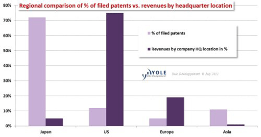
The number of patent applicants involved in SiC crystal/epiwafer technology totals about 350, located mainly in Japan (72%) and the USA (12%). The five main applicants (based on their number of patents) are Denso, Sumitomo, Nippon Steel, Bridgestone and Toyota (representing about 35% of the patents, collectively). The US firm Cree Inc ranks only 6th. However. this distribution is totally uncorrelated with the reality of the market, where 75% of SiC wafer business is generated by US-based companies, namely Cree, II-VI Inc and Dow Corning. Japan is only responsible for 5% of revenue (at least before the acquisition of Germany-based SiCrystal by Japan’s Rohm). Similar observations are seen in Europe and Asia (outside Japan) where patent-to-revenue ratio is currently very weak.
Japan leading in IP, but China and Korea taking off
Japan is has been increasingly involved in SiC technology since the 1980s. The USA was an early player and is still active. In contrast, only three Japanese companies are commercially active in SiC material: Showa Denko (epiwafers), Bridgestone (wafers) and Nippon Steel (wafers and epiwafers).
In the last five years, China and Korea have emerged as new players, with the establishment of companies in China such as Epiworld, TianYue, TYSTC, and Tankeblue, as well as Korea’s SKC. However, the market shares of these companies remains very low at the moment.

Figure 2.
SiC material: a question of expertise?
It seems obvious that IP considerations do not create a differentiating factor for success in the SiC substrate business. For example, Cree leads the industry with about 50% market share on a worldwide basis, and has the best reputation in terms of quality, diameter and reproducibility, says Yole. However, it does not own the widest patent portfolio. Thus, it seems that expertise and patent numbers do not correlate.
The only field where the number of patents and business size appears to be more balanced is for semi-insulating (SI) SiC technology, where both Cree (vanadium-free) and II-VI Inc (vanadium-doped) have extensively patented their respective developments.
How to enter the SiC substrate business?
The barriers to entry into the SiC substrate domain are very high: the current state-of-the-art stands at 6” diameter, with no micropipea and very low dislocation density. Only Cree seems to be able to offer such a product today, notes Yole. Why is this so?
First of all, over these last 20 years Cree has been widely funded by contracts from the US Department of Defense (DoD), Department of Energy (DoE), Defense Advanced Research Projects Agency (DARPA) and Navy, so it has been in a comfortable position for conducting much R&D and improving its technology for both LED and power electronics applications. So mastering SiC growth is probably a question of money, but also clearly a question of development time, which cannot be compressed. Yole says it seems reasonable then to think that there has been cross-fertilization between its LED and power electronics businesses that has allowed Cree to benefit from LED mass production (which is probably less stringent at the wafer level), fueling the power electronics side of the business. Finally, R&D efforts have never ceased, maintaining Cree’s lead, says Yole.
Apart from receiving funding to develop the technology, the only other options for quickly entering the SiC substrate sector appear to be through merger & acquisition (M&A) of an existing operation or through buying a license and related know-how (paying royalties in return). But which operations are for sale? Virtually nobody at this current time. Beyond the top five SiC substrate leaders, Yole does not see any clear positioning of firms that may want to participate in the sale or merger of their SiC business.
Ultimately, says the market research firm, attention should be paid to the new developments regarding LPE being made by Toyota, Denso or Sumitomo, as well as cubic-polytype 3C-SiC, which may disrupt the existing dominance of the PVT technique.


