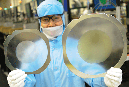
Cree Inc of Durham, NC, USA has announced the availability of high-quality, low-micropipe 150mm 4H n-type silicon carbide (SiC) epitaxial wafers, with highly uniform epitaxial layers as thick as 100 microns available for immediate purchase in limited quantities.

Cree reckons that this latest advance in driving the SiC materials marke to larger diameters will help to lower device cost and enable adoption for customers with existing 150mm-diameter device processing lines.
SiC semiconductor material is used in the production of a broad range of lighting, power and communication components, including LEDs, power switching devices and RF power transistors for wireless communications. Cree says that 150mm-diameter single-crystal SiC substrates enable cost reductions and increased throughput, while bolstering the continued growth of the SiC industry.
"Cree's ability to deliver high volumes of 100mm epitaxial wafers is unrivaled in the SiC industry, and our latest 150mm technology continues to raise the standards for SiC wafers," claims materials product manager Dr Vijay Balakrishna. "Our vertically integrated approach assures customers of a complete solution for high-quality 150mm SiC epitaxial wafers, providing industry leaders within the power electronics market the stable supply they demand," he adds.
Tags: Cree SiC epiwafers
Visit: www.cree.com
-->  --> Enter your search terms This Site Submit search a2a_linkname=document.title;a2a_linkurl=location.href;


--> Content on this page requires a newer version of Adobe Flash Player.

--> --> Content on this page requires a newer version of Adobe Flash Player.

-->


 ©2006-2012 Juno Publishing and Media Solutions Ltd. All rights reserved. Semiconductor Today and the editorial material contained within it and related media is the copyright of Juno Publishing and Media Solutions Ltd. Reproduction in whole or part without permission from Juno Publishing and Media Solutions Ltd is forbidden. In most cases, permission will be granted, if the magazine and publisher are acknowledged.
Disclaimer: Material published within Semiconductor Today and related media does not necessarily reflect the views of the publisher or staff. Juno Publishing and Media Solutions Ltd and its staff accept no responsibility for opinions expressed, editorial errors and damage/injury to property or persons as a result of material published.
Semiconductor Today, Juno Publishing and Media Solutions Ltd, Suite no. 133, 20 Winchcombe Street, Cheltenham, GL52 2LY, UK
Web site by No Name No Slogan 
var gaJsHost = (("https:" == document.location.protocol) ? "https://ssl." : "http://www."); document.write(unescape("%3Cscript src='" + gaJsHost + "google-analytics.com/ga.js' type='text/javascript'%3E%3C/script%3E")); try { var pageTracker = _gat._getTracker("UA-12169223-1"); pageTracker._trackPageview(); } catch(err) {}