Developers of system-on-chip(SoC)semiconductor devices need to add larger amounts of memory on chip and to support ever higher data rates.This is particularly true in image processing and communications.What are the options available?
SRAM:The simplest method of integrating RAM into SoCs is still the classic monolithic integration of SRAM blocks.By using the latest process technologies it is possible to integrate RAM capacities of significant size.For example,with a maximum RAM die area of 10mm2 the realistic limitations of the memory size are 16Mbit(65nm),32Mbit(40nm)and 64Mbit(28nm).Choosing the right configurations also allows for fast random access speeds.
A 32Mbit device could be configured in,say,64 blocks at 16Kwords x 32bit,resulting in a 2048bit access,which will allow data rates of 600Gbit/s at 300MHz.The"redundancy repair"concept allows for a yield optimisation within the SRAM integration process.
Embedded DRAM:Embedded DRAM has been a popular choice in previous process generations.However,the additional process options required for the monolithic integration of DRAM at feature sizes below 65nm has increased processing costs in a significant way.As a result,a number of companies,including Toshiba,no longer offer monolithically integrated DRAM technologies at 40nm and below.
DRAM Die in SiP:Where capacity demands cannot be met by integrated SRAM there is a trend towards DRAM-KGD(known good die)integration in SiP(system-in-package).Here DRAM die from qualified third-party manufacturers,who often specialise in this business,are placed on top of the logic die,bonded with bonding wires and integrated into a package;most often a BGA or QFP.
Current mainstream configurations are 64Mbit or 128Mbit with low-power or mobile DDR interfaces(16bit),or 16/32bit DDR2,which is mostly implemented with DRAM die manufactured in 65nm technology.
The next generation is dominated by 256/512Mbit DRAMs.The maximum realistic access bandwidth is currently around 25Gbit/s(DDR2 800Mbit/s,32bit interface).
When the engineers choose a DRAM die supplier they need to bear in mind that the usual life cycles of discrete DRAM components and SoCs with integrated DRAM dies often vary.It is important to assure the availability of the DRAM die across the entire production period.
Chip-on-chip:Engineers can work around the drawbacks associated with the commitment to one specific DRAM manufacturer during integration into a SiP by using CoC(chip-on-chip)technology.Here a soldering zone is set up for use at the surface of the logic/processor BGA package allowing a discretely packaged DRAM to be soldered onto this zone.
As the interface connections are short this set-up enables high bandwidth access to the DRAM with low power dissipation.Because the logic chip and the DRAM are purchased independently of each other another advantages is the option for multiple sourcing.
However,the design efforts associated with this package can be significant.So this approach is typically used in only very high-volumeapplications.
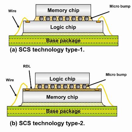
Stacked Chip SoC:For applications requiring a higher bandwidth than is achievable with SiP,another alternative is stacked chip SoC(SCS)technology.This uses specific DRAM die which are attached onto the logic chips through microbumps(bump-attach).These microbumps are all located in a single plane and with this set-up it is possible to implement up to several thousand connections.
As a result,the entire bit width of the internal RAM organisation(512-bits to 2048-bits,separate for read and write)can be connected through this interface directly with the logic chip's internal interface–without the conventional multiplexing into 16 or 32 external bits and without the necessity for any drivers,ESD protection structures and level shifters.
Present configurations in terms of capacity/interface are 512Mbit/512-bit,1Gbit/1024-bit and 2Gbit/2048-bit.At a single data rate interface speed of 160MHz,this results in maximum achievable bandwidths of 80Gbit/s,160Gbit/s and 320Gbit/s,respectively.
 Diode Surface Mount General Purpose Rectifier")


