Taiwan’s National Chung Hsing University has used nitride semiconductor growth on gallium nitride nanocolumns and nanoporosity achieved with photoelectrochemical etching to boost the light output power of light-emitting diodes (LEDs) by up to 1.75x [Ren-Hao Jiang et al, Appl. Phys. Express, vol6, p012103, 2013].
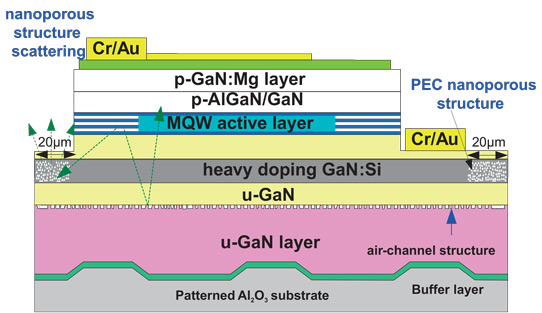
The researchers used metal-organic chemical vapor deposition (MOCVD) on patterned sapphire to grow the epitaxial material for the LEDs (Figure 1). The first two layers consisted of 30nm of low-temperature GaN (550°C) as a buffer, followed by 6μm of high-temperature undoped (u-)GaN (1150°C) as template.

Figure 1: Schematic structure of LED with nanoporous and air-channel regions (NA-LED).
The nanorod layer was formed using a 75Å-thick layer of nickel that was self-assembled into clusters by a rapid thermal anneal at 850°C in nitrogen for 90 seconds. The exposed GaN surface was reactive-ion etched. The nickel was removed by nitric acid solution, leaving nanorods that were 200-400nm in diameter and 0.5μm high.
The MOCVD process was then continued with 2μm of u-GaN (1150°C), 2μm of heavily doped n-GaN, 0.5μm of lightly doped n-GaN, a nine-period multi-quantum well layer (In0.2Ga0.8N/In0.01Ga0.99N, 3/13nm, 830°C), a six-period electron-blocking layer (Al0.3Ga0.7N/GaN, 2/2nm, 950°C), and, finally, 0.13μm of p-GaN.
The photoelectrochemical (PEC) process was preceded by cleaving the 2-inch wafer into two halves, and isolation using a triple-frequency ultraviolet Nd:yttrium aluminium garnet (355 nm) laser. The PEC etch process was performed with 0.5M oxalic acid, 0.5V DC bias, and illumination by a 400W mercury lamp. The PEC etch mainly attacked the heavily doped n-GaN layer, giving a nanoporous structure of ~0.1μm-diameter triangular holes. This region extended laterally about 20μm into the n-GaN layer from the laser scribe line. The PEC etch also reduced the diameters of the nanorods in the air-channel region.
Various LEDs were produced with/without air-channels from the nanorods, and with/without nanoporous regions from the PEC. The p-GaN layer was covered with 250nm of indium tin oxide (ITO) transparent conductor. The n- and p-type metal contacts consisted of chromium/gold.
The peak emission wavelength at 20mA for the LED with air-channels and nanoporous regions (NA-LED) was 438.7nm (Figure 2a). The peaks for standard (ST-LED) and air-channel (A-LED) LEDs were both at 439.5nm. The line-widths for all LEDs were around 16nm.

Figure 2: EL emission-peak wavelengths of LEDs measured at 20mA. (b) Operation voltage and light output power versus injection current. (c) Far-field radiation patterns of the LED structures at 20mA. (d) Light-enhancement ratios of A-LED and NA-LED measured by varying detection angle.
The operating voltage at 20mA was also the same over the devices at 3.05V (Figure 2b). However, the NA- and A-LEDs had 1.75x and 1.48x the output power of the ST-LED. The researchers attribute the improvements to better light scattering leading to increased light extraction from the devices.
The air-channels and nanoporosity also led to narrower light beams, with a divergence angle of 122° for the NA-LED, compared with 138° for the A-LED and 146° for the ST-LED (Figure 2c).


