Strategies United predicts that by 2015 the global market for high brightness LEDs (HB-LEDs) will generate revenues of $18.9 billion, representing a compound growth rate of 11.8%. A key factor in the growth of HB-LEDs is the use of patterned sapphire substrates (PSS) to enhance light extraction efficiency. PSS’s demanding metrology requirements can have a major impact on wafer yield. Specialized 3D optical microscopes can quantify the height, width and pitch of PSS features on production wafers and readily spot defective features with greater speed and, hence, higher sampling ratios than other techniques. The end result in many cases is a substantial increase in yield that can pay back the cost of the instrument in a short period of time.
PSS background
Over the last several years, HB-LEDs have penetrated a number of new market applications such as display chips and solid-state lighting. A key factor in growth of HB-LEDs is the use of PSS to increase light extraction efficiency. The PSS technique consists of etching a repetitive grid structure into the sapphire to scatter light confined in the Gallium Nitride (GaN) layer. Besides increasing light extraction efficiency, PSS structures reduce dislocation defect density in the GaN layer, resulting in improved efficiency. As a general rule, the smaller the feature size of the grid structure, the greater the improvement in light extraction efficiency. Obtaining maximum efficiency for the reflector requires achieving consistent PSS grid geometry.
Dry etching is the most common method for producing PSS wafers. A layer of photoresist is deposited onto the sapphire substrate. Lithography exposes a step pattern onto the photoresist. Exposure to fluoride-based plasma gas and microwave energy anisotropically etches the crystalline structure to form a dense, uniform patterned of cones or pyramids. Dry etching rates typically run in the order of 50 to 200 nanometers (nm) per minute, and a standard 2-inch wafer typically takes between 30 and 60 minutes to etch.
Role of metrology
Metrology tools play a critical role by ensuring PSS structures are created with the right height, width and pitch. The gold standard for PSS shape measurement is the atomic force microscope (AFM), which is widely used by both wafer suppliers and LED manufacturers because it can directly measure the entire PSS surface, even where it is steeply sloped. In atomic force microscopy, a sharp probe is brought into close proximity to a sample. Probe and sample are subsequently moved relative to each other in a raster pattern, and a quantity is measured in a serial fashion at discreet locations. Interaction between the tip and sample is measured by monitoring the displacement of the free end of the attached cantilever.
Substrate wafer suppliers typically utilize the AFM to measure the smoothness of the wafer after the polishing process and to spot film defects in epitaxial layers. They also use the AFM to provide the dimensional characterization of the PSS at atomic resolution. Dedicated instruments of this type play a critical role in both research and development and production applications by performing automated measurement, data collection, data analysis and report generation on PSS wafers.
However, wafer suppliers involved in production applications usually require greater measurement speed than can be achieved by an AFM. It typically takes these instruments several minutes to process a single site on the wafer, and wafer suppliers typically need to process 5 to 10 locations per wafer depending on wafer size and feature specifications. AFM measurement speed typically limits the proportion of wafers that can be sampled. Thus, a process deviation that causes out of specification wafers to be produced may not be detected until a considerable number of bad wafers have been etched. Wafers that have not been correctly patterned need to undergo re-polish, which reduces the thickness of the wafer to the point that it cannot go through the patterning process again. The wafer normally must be sold as an unpatterned sapphire substrate at a considerably lower selling price.
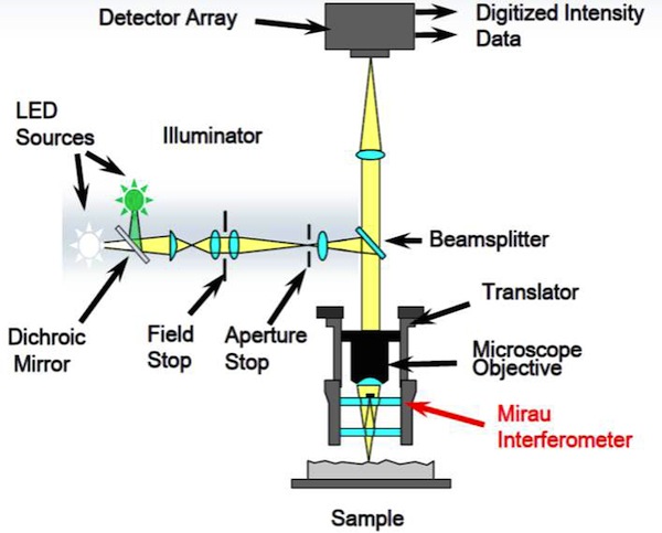
Figure 1: Operation of 3D optical microscope.
Value of 3D optical microscope
A 3D optical microscope based on interferometry improves PSS yield by substantially reducing the time required to make 3D measurements. More wafers can be tested in more locations over less time to detect process problems faster. The 3D optical microscope captures 3D surface measurements based on a technique called white light interferometry. Light approaching the sample is split and directed partly at the sample and partly at a high-quality reference surface. The light reflected from these two surfaces is then recombined. Where the sample is near focus, the light interacts to form a pattern of bright and dark lines that track the surface shape.
The microscope is scanned vertically with respect to the surface so that each point of the test surface passes through focus. The location of the maximum contrast in the bright and dark lines indicates the best focus position for each pixel. This allows the microscope’s computer to obtain a full 3D profile over the entire field of view of the camera as the sample is quickly and automatically stepped through focus. The entire data acquisition and analysis is completed in just a few seconds.
3D optical microscopes have been optimized specifically for PSS applications. A rugged design with continuous self-calibration enables these systems to quickly measure sub-nanometer roughness of substrates over several square millimeters, even in noisy production environments. The instrument can be configured to measure wafers ranging from 2 to 8 inches in diameter at any desired number of locations. In comparison to an AFM, the time required to measure each location is reduced from a few minutes to a few seconds, with comparable results for both surface roughness and PSS height and width.
The 3D optical microscope often makes it practical to increase the number of measurement locations and provides a higher level of confidence that the measurements are representative of the entire wafer surface. Integrated with a wafer handling system, this quality control tool supports turnkey operation for production quality assurance/quality control environments and seamless integration with automated substrate handlers.
3D optical microscope measurements
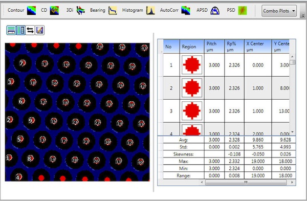
Figure 3: PSS regions measured by 3D optical microscopy are automatically identified and key features automatically reported.
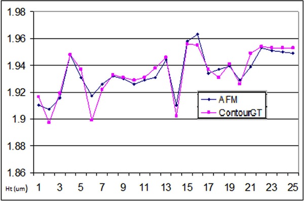
Measurements generated by a 3D optical microscope correlate very well with AFM measurements. Figure 4 shows a series of measurements of peak height taken at the same location on 25 different wafers with an AFM and a 3D optical microscope. The greatest difference between the two measurements is less than 0.02 microns. The 3D optical microscope provides vertical resolution of better than 0.02 nanometers on a range of feature heights up to 10 millimeters. In the horizontal plane, a 3D optical microscope can image features as small as 130 nanometers.
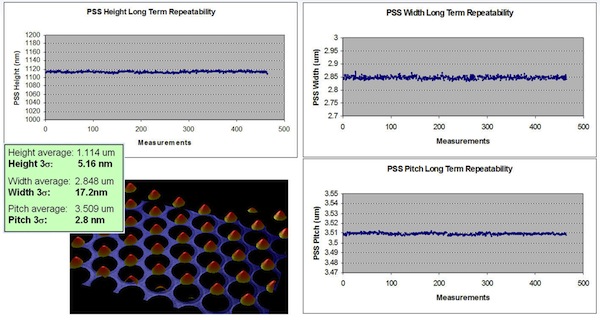
3D optical microscopes also provide excellent repeatability, especially when employing the continuous calibration option available for production systems. Figure 5 shows that measurements of PSS height that averaged 1.114 microns exhibited a 3σ repeatability of 5.16 nanometers on a series of 480 measurements taken over several days. Likewise, measurements of feature width averaging 2.848 microns showed a 3σ repeatability of only 17.2 nanometers. Average pitch dimension was 3.509 microns and 3σ repeatability was only 2.8 nanometers.
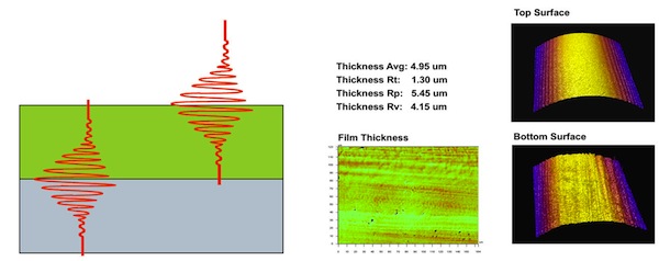
3D optical microscopes can also be used to measure photoresist layer thickness, another important process variable in the production of PSS wafers. Film thickness software that works with the microscope reports the height of the top surface of the film, the height of the top surface of the substrate and the film thickness. This approach works for single layer films from about 1.5 microns to 800 microns in thickness, depending on film material. Unlike confocal microscopes, 3D microscopes using interferometry provide the same vertical resolution independent of magnification, so thickness measurements can be made over large areas for maximum statistical significance.
A 3D optical microscope can generate a substantial return on investment by increasing PSS wafer yield. For example, a wafer manufacturer produces about 100,000 wafers per month. The company originally operated at about an 80% yield with 20,000 wafers per month having to undergo re-polish due to PSS issues. Each of these wafers costs $1 for re-polish plus a $2 reduction in sales price of a second-grade wafer. Purchase of a 3D optical microscope increased the yield to 90% by making it possible to inspect a higher proportion of wafers and completing the inspection on a more timely basis so that problems were identified and could be corrected sooner. The result was that yield increased to 90%, saving about $30,000 per month. This savings was enough to pay for the cost of the optical microscope in less than one year.
The seamless integration of 3D microscope process monitoring within the PSS production environment requires more than just performance and speed. Automated wafer handling, technician-level software operation, and customizable statistical analysis and archiving also are absolute requirements. The latest generation of 3D optical microscopes enables highly repeatable, high-throughput, nanometer-surface metrology of HB-LED PSS.


