Diodes, in general, are made of very thin layers of semiconductor material; one layer will have an excess of electrons, while the next will have a deficit of electrons. This difference causes electrons to move from one layer to another, thereby generating light. Manufacturers can now make these layers as thin as .5 micron or less (1 micron = 1 ten-thousandth of an inch).
Impurities within the semiconductor are used to create the required electron density. A semiconductor is a crystalline material that conducts electricity only when there is a high density of impurities in it. The slice, or wafer, of semiconductor is a single uniform crystal, and the impurities are introduced later during the manufacturing process. Think of the wafer as a cake that is mixed and baked in a prescribed manner, and impurities as nuts suspended in the cake. The particular semiconductors used for LED manufacture are gallium arsenide (GaAs), gallium phosphide (GaP), or gallium arsenide phosphide (GaAsP). The different semiconductor materials (called substrates) and different impurities result in different colors of light from the LED.
Impurities, the nuts in the cake, are introduced later in the manufacturing process; unlike imperfections, they are introduced deliberately to make the LED function correctly. This process is called doping. The impurities commonly added are zinc or nitrogen, but silicon, germanium, and tellurium have also been used. As mentioned previously, they will cause the semiconductor to conduct electricity and will make the LED function as an electronic device. It is through the impurities that a layer with an excess or a deficit of electrons can be created.
To complete the device, it is necessary to bring electricity to it and from it. Thus, wires must be attached onto the substrate. These wires must stick well to the semiconductor and be strong enough to withstand subsequent
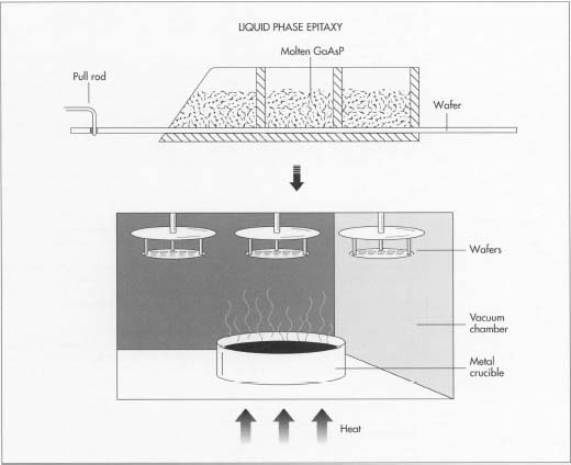
Contact patterns are exposed on the wafer's surface using photoresist, after which the wafers are put into a heated vacuum chamber. Here, molten metal is evaporated onto the contact pattern on the wafer surface.
processing such as soldering and heating. Gold and silver compounds are most commonly used for this purpose, because they form a chemical bond with the gallium at the surface of the wafer.
LEDs are encased in transparent plastic, rather like the lucite paperweights that have objects suspended in them. The plastic can be any of a number of varieties, and its exact optical properties will determine what the output of the LED looks like. Some plastics are diffusive, which means the light will scatter in many directions. Some are transparent, and can be shaped into lenses that will direct the light straight out from the LED in a narrow beam. The plastics can be tinted, which will change the color of the LED by allowing more or less of light of a particular color to pass through.
Design
Several features of the LED need to be considered in its design, since it is both an electronic and an optic device. Desirable optical properties such as color, brightness, and efficiency must be optimized without an unreasonable electrical or physical design. These properties are affected by the size of the diode, the exact semiconductor materials used to make it, the thickness of the diode layers, and the type and amount of impurities used to "dope" the semiconductor.


