New LED Technology
There are two competing technologies which could radically change the nature of lighting in the future: OLEDs and PLEDs.
- Organic Light Emitting Diodes (OLEDs) are based on multiple layer devices (up to 16 layers) of evaporated low molecular weight molecules.
- Polymer Light Emitting Diodes (PLEDs) are solution processible structures based on a single white light emitting polymer, deposited by printing on to charge transport layers, typically PLEDs are 3 or 4 layers thick
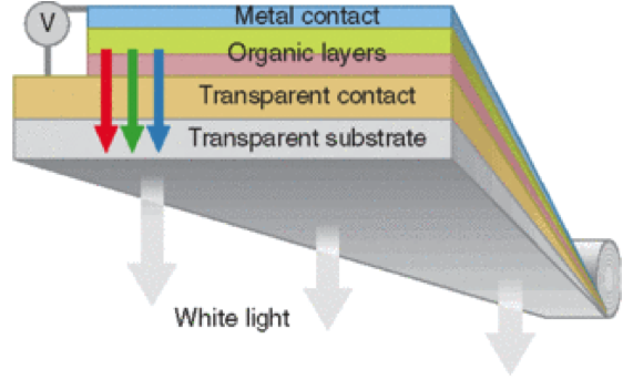
Figure 1 depicts a cross-section through both structures. Both devices represent extended emissive surfaces with devices up to 1/5 m2 already being demonstrated from the laboratory. However in general, laboratory-made devices are much smaller - generally 10's of square centimetres in area. The main research effort continues within the materials, striving for improved quality of white light, lifetimes and efficacy. Presently OLEDs outperform PLED technology, on laboratory test samples, but due to the complexity of manufacturing multiple layer structures it is widely believed that solution processible PLED technology will be first to demonstrate high direct yield manufacturing levels.
OLEDs
If the emitting layer material of the LED is an organic compound, it is known as an Organic Light Emitting Diode (OLED). So far, OLEDs are intrinsically well suited for indoor area illumination and could appear as 'glowing wall paper' or 'illuminated ceiling tiles' without the need for 'luminaires'.
OLEDs utilise flat display technology and are made by placing a series of organic thin films between two conductors. When electrical current is applied, a bright light is emitted. OLED's could tackle in the future the material and production challenges currently encountered with SSL LEDs. OLEDs are already on the market for particular, very flat illuminated displays in portable devices. Television manufacturers are still weighing up the benefits of OLEDs over LEDs (i.e. for flat panel LED TVs). OLEDs based on organic material are still under development. OLED efficiencies under particular operational conditions have been reported up to 64 lm/W at 1000 Cd/m² but still have to prove their efficacy in actual working conditions (e.g. temperature and life).
PLEDs
PLEDs consist of thin, flexible film made of polymers and capable of emitting the full color spectrum of light. These solution processed light emitting devices are simple 'few layer' devices based on polymeric functional materials. The active polymers serve a dual role in transmitting the charge and also converting it into light. The ability to dissolve the active materials (Hole Injection/Transport Layer, Interlayer/Primer Layer and Light Emitting Polymer) in a solvent to form an "ink" and deposit by a range of printing techniques on a wide variety of substrates at low temperatures provides a number of manufacturing advantages over small molecule OLED technology.
The best devices are currently achieving > 30lm/W with a half life of ~30Khrs at 500 Cd/m². It is expected that by 2011, PLED devices will exhibit > 60lm/W with 70% life being > 20K hrs. These materials emit no UV or IR and the expected thermal uplift, for a 600 sq tile fitting, is <15oC.
A PLED has 4 main layers:
1. A glass or plastic substrate - for PLED fabric displays, plastic tends to be a better choice because it's less fragile but more flexible than glass.
2. A transparent electrode coating, which is applied to one side of the substrate
3. The same side of the substrate is then coated with the light emitting polymer film
4. The final layer is an evaporated metal electrode, which is applied to the other side of the polymer film
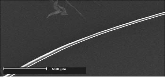
PLEDs are a good example of 'nanotechnology'.The total thickness of all layers in a PLED display device can be less than 500nm.Human hair 0.1mm thick

Human hair 0.1mm thick

Organic layer thickness 1/2000 a human hair!!
0.00005mm (50nm)
Controlled layer thickness to 10% (5nm)


