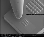
The MicroLEDs semiconductor manufacturing process includes construction of a parabolic reflector to enable optimal light control and high efficiency from micro-meter-sized LEDs.
InfiniLED has announced new output-power achievements from its MicroLEDs process that combine characteristics of both LED and lasers. The latest devices produce 1 mW of radiant power from a single 20-μm emitter with a wavelength of 405 nm. InfiniLED says that the technology will soon be commercialized in products such as medical devices or screen backlighting.

The company said that the 1-mW achievement is the equivalent of light output density greater than 300 W/cm2. Specifically, the company said the density was "the highest recorded for a commercially available LED type device."
The MicroLED is built using an LED semiconductor structure and can be driven like standard LEDs. But the manufacturing process, which includes etching of a parabolic reflector at the semiconductor level, delivers a collimated beam like a laser (see the parabolic structure in the nearby photo). The result is both high-intensity light and high efficiency.
"This device can be seen as a cross-over between the power and collimation of a laser and the simplicity of an LED. The unique devices enable a range of applications," said chief commercial officer of InfiniLED, Bill Henry. "InfiniLED are proud to have achieved the landmark performance of optical density greater than 300 W/cm2. This was achieved without the need for external optics indicating the potential for further improvement of the performance."
InfiniLED plans to manufacture the MicroLEDs in single-pixel and cluster configurations, and in the latter case optionally offer addressable control of each pixel. The company has said that low capacitance allows the LEDs to be switched on and off at very high speed.
The company has identified a number of applications for the MicroLEDS, including usage as a backlight in small display applications such as battery-powered consumer electronics. The small size will also enable medical and life-science applications because the LEDs can be embedded in tiny place. The nearby photo shows a 25-LED array alongside the tip of a needle. Other potential applications include printing and lithography.


