Fujitsu Laboratories of Kawasaki, Japan has developed compact gallium nitride high-electron-mobility transistor (HEMT)-based transceiver module technology with an output of 10W operating at frequencies up to the millimeter-wave band.
Until now, developing high-output modules that operate in the millimeter-wave band has required modules consisting of separately packaged components to allow sufficient heat dissipation. Consequently, it has been difficult to produce compact modules. In addition, because signal loss tends to increase in internal module terminal connector components at higher frequencies, reaching millimeter-wave operations has proven to be challenging.

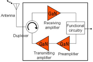
Figure 1: Diagram of millimeter-wave GaN transceiver module.
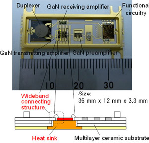
Fujitsu's new high-output millimeter-wave transceiver module features a new heat-sink structure embedded into multilayer ceramic substrate technology. Compared to previous designs, heat dissipation improved by a factor of five times, enabling 10W-class output levels.
Fujitsu devised a wideband connector structure that reduces loss at higher frequencies in the heat sink. With the new input/output connector structure, high-frequency signals passing through the module can be transmitted at up to 40GHz (twice the frequency levels of previous designs).
It was possible to shrink the size of the millimeter-wave transceiver module. With dimensions of 12mm × 36mm × 3.3mm, the new module is less than 1/20 the size of conventional integrated units.

Figure 2: Photo and structure of millimeter-wave GaN transceiver module.
As well as being used as a material in blue LEDs, gallium nitride (GaN) features a relatively high electron transfer rate and resistance to voltage-induced breakdown compared to conventional semiconductor materials such as silicon and gallium arsenide (GaAs). Therefore Fujitsu Laboratories comments that GaN HEMTs show promise for supporting high-output, exceptionally efficient operation.
With the new technology, it is possible to combine multiple chips in a single unit, enabling the development of more compact and lighter equipment with improved performance for wideband communications and radar systems. Details of the new technology were first presented at the IEEE MTT 2013 International Microwave Symposium (IMS 2013) at the beginning of June in Seattle, WA, USA.
Market potential
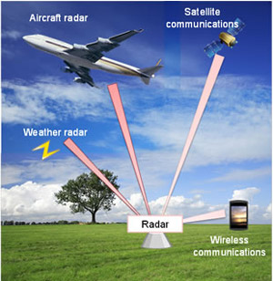
In line with the progression of an increasingly network-based society, radio-wave demand in a variety of wireless systems is expected to increase even further, Fujitsu contends. For example, in the field of smart-phones and other wireless communications, there is a shortage of available frequencies.
Using millimeter waves to accommodate this increase in demand is being given consideration. Likewise, aircraft currently employ the 10GHz frequency band, but a move toward the usage of higher frequencies is expected to take place in the future.

Figure 3: Usage scenarios for the millimeter-wave band.
Current generations of high-output millimeter-wave transceiver modules typically consist of separately packaged transmitter and receiver components. Being able to integrate both functions in a single unit, however, will enable equipment to become more compact.
Furthermore, transceiver modules needed for millimeter-wave communications and radar require wideband capabilities for operating in the millimeter-wave band, as well as high-output performance sufficient to cover wide geographic areas. Fujitsu adds that, when developing a transceiver module with 10W-class high-output power, "it is critical to improve the transceiver module's heat dissipation characteristics, as heat generation intensifies in tandem with higher output levels.
Moreover, it is also necessary to reduce signal loss in connector components. This is because, at higher frequencies, loss increases in the components connecting the chip and the wiring that transmits a signal.


