Researchers in Japan have created indium phosphide (InP) nanowire (NW) solar cell structures with internal quantum efficiencies (IQEs) that beat the performance of bulk InP-based devices in the short-wavelength range of 300-570nm [Masatoshi Yoshimura, et al, Appl. Phys. Lett., vol103, p243111, 2013].
The InP nanowires had a single p-type doping profile. The photovoltaic junction arose from the further deposition of indium tin oxide (ITO) as a transparent electrode. By growing nanowires with only p-InP, rather than a p-InP/n-InP junction, the researchers say that the process is potentially more controllable and less costly.
The work was carried out by Hokkaido University and Japan Science and Technology Agency (JST).
The p-type InP nanowires were grown using selective-area metal-organic vapor phase epitaxy (SA-MOVPE) on p-type InP substrates. The selective-area mask consisted of 20nm silicon dioxide patterned with 200nm-diameter holes in a triangular array of 400nm pitch in an area of 1.2mm x 1.2mm. After the growth of the nanowires out of the holes in the mask, they were embedded in spin-coated benzocyclobutene (BCB) from Dow Chemical.
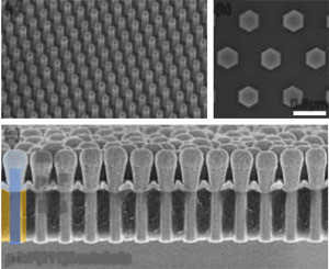
The ITO was rf sputtered after the nanowire tips were exposed by etching back the BCB. U-shaped metal electrodes consisted of silver on the ITO and gold-tin on the back-side of the substrate. The effective area of the device was 0.62mm2. This area contained 4.5x10⁶ nanowires that filled about 18% of the geometric area of the device (Figure 1).
 Figure 1: (a) 20°-tilted view scanning electron micrograph (SEM) of p-InP NW array. (b) Top-view SEM of NWs. (c) SEM cross-section of ITO/p-InP heterojunction NW solar cell.
The researchers believe the deposition process of ITO as the transparent conductor layer forms an n+ defect region near the surface, giving a ‘buried n+/p homojunction’.
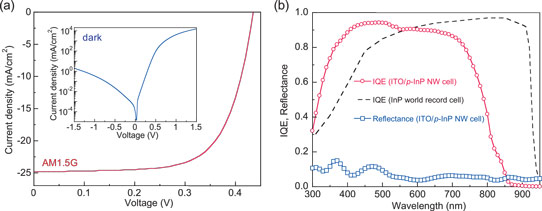
Under AM1.5G solar illumination (Figure 2), the open-circuit voltage (Voc) was 0.436V, the short-circuit current density (Jsc) was 24.8mA/cm2, and the fill factor (maximum power density/VocxJsc) was 0.682. The overall power conversion efficiency was 7.37%. Planar ITO/InP solar cells have achieved 18.9% efficiency.

Figure 2: (a) Illuminated current-voltage (J-V) characteristics of TO/p-InP NW cell under AM1.5G. Inset: dark J-V characteristics (semilog scale). (b) IQE and reflectance of ITO/p-InP NW cell. Also included is IQE of InP world record planar cell.
Considering that 82% of the active area of the device was space between the wires, “this high Jsc for a NW-array-based device resulted from the combination of near-field-optics enhanced absorption and anti-reflection effects,” the researchers comment. Although there was no anti-reflective coating, the device had an effective reflectance of only 6.2%.
Investigation of IQE gave a value of more than 80% in the 400-750nm range. The researchers write: “The IQE at shorter wavelengths was much higher than the previous reported InP NW solar cell, and the device had peak IQE of 0.943 at 490nm without employing a window layer for reflecting minority carriers moving toward the front ITO layer.”
The IQE in the range 300-570nm beat that of the record holder for a planar InP structure. The researchers attribute this to reduced surface recombination, and to improved separation and collection of photogenerated carriers. The reduced recombination was a result of minority carrier reflection by the wide-bandgap ITO window layer. The more efficient separation/collection was due to a junction forming also on the sides of the nanowires as a result of the ITO forming hemispherical caps.
The researchers estimate that light with wavelength shorter than 500nm was absorbed within 300nm in their InP nanowires. The absorption edge on the long-wavelength/low-energy side is somewhat blue-shifted to 870nm from the 925nm bandgap of bulk InP. Selective-area electron diffraction (SAED) patterns in a high-resolution transmission electron microscope (HR-TEM) system suggest that the nanowires have a wurzite structure, which has a bandgap that is about 80meV wider than that of the zincblende structure usual with bulk InP. A wider bandgap would lead to blue-shifting of the absorption edge.