Meijo and Nagoya universities in Japan have developed a laser lift-off (LLO) technique for removing gallium nitride (GaN) substrates from ultraviolet (UV) light-emitting diodes (LEDs) to improve light extraction efficiency [Daisuke Iida et al, Appl. Phys. Lett., vol105, p072101, 2014].
GaN substrates absorb UV-A light due to impurities such as oxygen and carbon. Typical LLO techniques use UV laser light to separate GaN buffer layers from sapphire substrates. The UV light is strongly absorbed by the GaN layers but not by the sapphire. The absorbed light decomposes the GaN structure and droplets of Ga form, allowing separation of the GaN from sapphire.
However, UV LED devices cannot be separated in this way since the UV laser light would also damage the UV active region. The Meijo/Nagoya team has instead developed an LLO technique for devices grown on free-standing GaN substrates which uses visible laser light absorbed by a superlattice with gallium indium nitride (GaInN) layers. The visible laser light does not damage the UV emitting layers. The use of free-standing GaN substrates reduces the density of performance-killing threading dislocations, also improving performance.
The heterostructures were produced by metal-organic vapor phase epitaxy in a face-down 2-inch x 3-wafer horizontal-flow reactor. The substrate was free-standing GaN, with a threading dislocation of density less than 106/cm2. The researchers first developed the LLO technique involving Ga0.85In0.15N/GaN superlattice (SL) structures that would act as 'removing layer'.
Samples with and without the removing layer were grown. The removing layer, where present, was sandwiched by 1μm n-GaN layers ('Sample A'). In the comparison sample (B) without removing layer, a 1μm n-GaN layer was grown on the free-standing substrate. The samples were completed by 2μm of n-Al0.03Ga0.97N.
The GaInN material is unstable at high temperature and decomposes with indium droplets forming at high temperature, such as the 1040°C used to grow the n-GaN and n-AlGaN layers. The threading dislocation density of sample A with removing layer increased to 5x10⁷/cm2, while sample B without removing layer showed a smaller increase to 3x10⁶/cm2.
The researchers comment: "We consider that, after the decomposition of Ga0.85In0.15N/GaN SLs during growth, the threading dislocations were induced via the generation of misfit dislocation in the interface between n-GaN and the In droplet layer."
This would lead to expectations of reduced LED performance for devices grown on sample A templates. However, the dislocation densities in both samples were still lower than the values that are typical in nitride semiconductors grown on sapphire (2-5x10⁸/cm2).
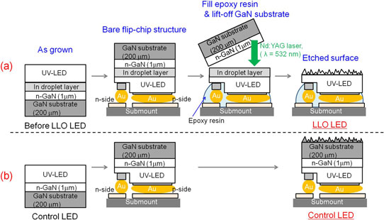
Having developed the LLO method, the researchers produced 380nm UV-A LEDs to test its suitability (Figure 1). The removing layer consisted of an 8-period SL. Above the removing layer were 1μm of n-GaN, 2μm of n-AlGaN, a 10-period 2nm/2nm Ga0.97In0.03N/GaN SL, a 10-period 6nm/12.5nm Ga0.95In0.05N/GaN multiple quantum well (MQW) active region, a 20nm p-Al0.13Ga0.87N electron-blocking layer, and a 120nm p-GaN contact.

Figure 1: Schematic view of fabrication steps of (a) LLO and (b) control LEDs.
Fabrication consisted first of plasma etch down to the n-AlGaN contact layer, deposition of silver/indium tin oxide (ITO) n- and p-contacts, singulation into 500μmx600μm chips, flipping onto submounts with gold bumps, and epoxy resin fill of the gap between chip and submount.
Next came the LLO step using a pulsed second-harmonic 532nm Nd:YAG laser with irradiation energy density of 125mJ/cm2. Tests suggested that the SL removing layer that had decomposed into indium droplets absorbs visible light through surface plasmon resonance. By contrast, the GaN substrate and UV LED layers do not absorb visible light. Therefore, the laser light is selectively absorbed by the removing layer, allowing lift-off. The device layers were thus not damaged by high-energy visible laser light, as often happens in other LLO processes.
Finally, the emission surface of the LED was roughened with an etch process in hot potassium hydroxide solution. Such roughening can increase light extraction efficiency.
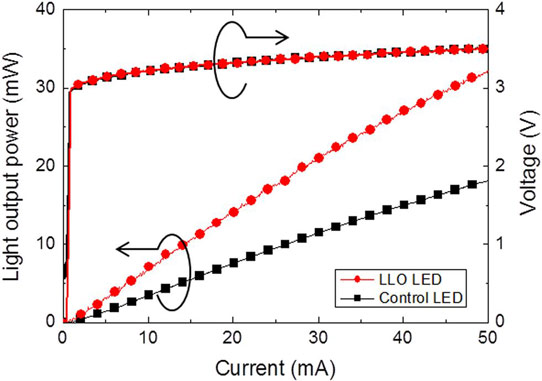
Although the LLO device was expected to have reduced internal quantum efficiency (IQE) due to the higher threading dislocation density of the template, the higher light extraction efficiency results in brighter emission compared with a control device produced on a sample B template. Also, the peak wavelength of the LLO LED was slightly shorter at 380nm, compared with 383nm for the control. The thick GaN substrate absorbs shorter wavelengths more strongly, shifting the peak to longer wavelengths.

Figure 2: Light output and voltage versus current characteristics of LLO and control LEDs.
At 50mA, the output power of the LLO LED was 1.7x that of the control (Figure 2). At the same time, the current versus voltage performance of the two devices was very similar. The researchers attribute this to the extremely low resistance of the n-AlGaN contact.


