A research team led by faculty scientist Ali Javey at the US Department of Energy's Lawrence Berkeley National Laboratory (Berkeley Lab) has created a transistor with a gate length (the defining dimension of a transistor) just 1nm long, which is the smallest reported to date ('MoS2 transistors with 1-nanometer gate lengths', Science Vol. 354, Issue 6308, p99-102).
For conventional semiconductors, the laws of physics set a 5nm threshold on the size of transistor gates (about a quarter the size of high-end 20nm-gate transistors currently on the market). However, the 1nm-gate transistor show that "with the choice of proper materials, there is a lot more room to shrink our electronics," says Javey, lead principal investigator of the Electronic Materials program in Berkeley Lab's Materials Science Division (and a University of California Berkeley professor of electrical engineering and computer sciences). The key was to use carbon nanotubes and molybdenum disulfide (MoS2).
Other investigators on the paper include Jeff Bokor, a senior faculty scientist at Berkeley Lab and a professor at UC Berkeley; Chenming Hu, a professor at UC Berkeley; Moon Kim, a professor at the University of Texas at Dallas; and H.S. Philip Wong, a professor at Stanford University.
The new development could be key to keeping alive Intel co-founder Gordon Moore's prediction that the density of transistors on integrated circuits would double every two years.
"The semiconductor industry has long assumed that any gate below 5nm wouldn't work, so anything below that was not even considered," says study lead author Sujay Desai, a graduate student in Javey's lab. "This research shows that sub-5nm gates should not be discounted. Industry has been squeezing every last bit of capability out of silicon. By changing the material from silicon to MoS2, we can make a transistor with a gate that is just 1nm in length, and operate it like a switch."

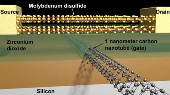
Picture: Schematic of transistor with a MoS2 channel and 1nm carbon nanotube gate. (Courtesy of Sujay Desai/Berkeley Lab.)
Both silicon and MoS2 have a crystalline lattice structure, but electrons flowing through silicon are lighter and encounter less resistance compared with MoS2. That is a benefit when the gate is 5nm or longer, but below that length the quantum mechanical phenomenon of tunneling kicks in and the gate barrier is no longer able to keep the electrons from barging through from the source to the drain terminals. "This means we can't turn off the transistors," says Desai. "The electrons are out of control."
Because electrons flowing through MoS2 are heavier, their flow can be controlled with smaller gate lengths. MoS2 can also be scaled down to atomically thin sheets (about 0.65nm thick) with a lower dielectric constant (reflecting the ability of the material to store energy in an electric field). Both of these properties, in addition to the mass of the electron, help to improve the control of current flow inside the transistor when the gate length is reduced to 1nm.
For constructing the transistor's gate, conventional lithography techniques do not work well at a scale of 1nm, so the researchers turned to hollow cylindrical carbon nanotubes with diameters as small as 1nm. They then measured the electrical properties of the devices to show that the MoS2 transistor with the carbon nanotube gate effectively controlled the flow of electrons.

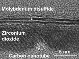
Picture: Transmission electron microscope image of a cross-section of the transistor, showing 1nm carbon nanotube gate and molybdenum disulfide semiconductor separated by the insulator zirconium dioxide. (Courtesy of Qingxiao Wang, UT Dallas.)
"However, it's a proof of concept. We have not yet packed these transistors onto a chip, and we haven't done this billions of times over," notes Javey. "We also have not developed self-aligned fabrication schemes for reducing parasitic resistances in the device. But this work is important to show that we are no longer limited to a 5nm gate for our transistors. Moore's Law can continue a while longer by proper engineering of the semiconductor material and device architecture."
The work at Berkeley Lab was funded primarily by the Department of Energy's Basic Energy Sciences program.