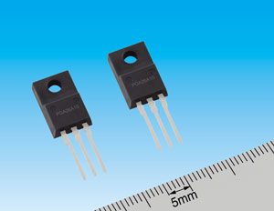
Panasonic Corp of Osaka, Japan has announced the development of a gallium nitride (GaN)-based power transistor with a blocking voltage of 600V that enables stable switching operations. Shipment of evaluation samples began in March.
The firm claims that its design will for the first time ensure ‘failure-free operation’ by 600V GaN power transistors. The GaN transistors, housed in a small-size package, are also said to contribute to saving energy in a variety of power switching systems for both industrial and consumer applications.

Picture: Panasonic’s 600V GaN gate injection transistors.
The new GaN transistor has the following three key technical features:
Normally-off gate injection transistor on 6-inch silicon substrate
Power switching systems require normally-off operation of such transistors for safe operation. Lowering the cost of the substrate for growing GaN-based films is also required for GaN transistors to be cost-effective. Panasonic claims that it has solved these issues through its novel design of normally-off gate injection transistors (GITs) developed on cost-effective silicon substrates.
Proprietary technologies for the epitaxial growth of GaN by metal-organic chemical vapor deposition (MOCVD) enable the fabrication of GaN transistors on a 6-inch silicon substrate. The p-type gate of the GIT reduces on-state resistance by taking advantage of conductivity modulation by the hole injection from it.
Stable switching operation free from current collapse
Up to now, the increase in on-state resistance after the application of high-voltage current collapse has been a serious problem for commercializing GaN transistors. This increase is the greatest obstacle to achieving stable operation.
The origin of current collapse is believed to be trapped electrons under a high electric field. Panasonic says that, through its novel processing technologies and new device structures that relieve the electric field, it has reduced the number of traps. The gate injection transistor fabricated on silicon enables stable 600V operation free from current collapse.
Highly efficient switching at high frequencies
The lateral structure of the gate injection transistor is advantageous for high-speed switching due to lower parasitic capacitance than is typical of conventional silicon-based power transistors with their vertical structures. Here, RonQg (where Ron is on-state resistance and Qg is gate charge) is a figure-of-merit for high-speed switching. The newly fabricated gate injection transistor exhibits a low RonQg of 715mΩnC, which is 7.5% lower than that achieved by ‘state-of-the-art’ silicon MOS transistors.
Also, by using the gate injection transistors on silicon, Panasonic has demonstrated 1MHz operation of resonant LLC DC-DC converters at an efficiency above 96%.
Panasonic says this demonstration indicates that the transistor can be used for practical systems free from operational failure. Applications for 130 domestic and 112 overseas patents have been filed.
The research results were presented at the Applied Power Electronics Conference (APEC 2013) in Long Beach, CA, USA (17-21 March). The work has been partially supported by the New Energy and Industrial Technology Development Organization (NEDO), Japan, under the Strategic Development of Energy Conservation Technology Project.


