University of California Los Angeles (UCLA) has developed gallium antimonide (GaSb) thermophotovoltaic (TPV) cells on gallium arsenide (GaAs) substrates [Bor-Chau Juang et al, Appl. Phys. Lett., vol106, p111101, 2015]. The use of GaAs rather than more expensive, smaller GaSb substrates should allow lower-cost production of such devices. GaSb is presently limited to diameters less than 4-inches, while commercial 6-inch GaAs substrates are available.
TPV devices typically target thermal radiation in the 1000°C range with wavelengths of 1.6-2.3μm for conversion of waste heat into electrical power. A large number of compound semiconductors have bandgap energies that fall in this range (0.54-0.78eV). However, lattice matching can be a problem, restricting material compositions and allowed wavelength ranges. The indium gallium arsenide antimonide (InGaAsSb) family of materials is lattice matched to GaSb, avoiding such constraints.
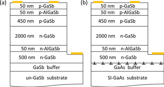
Growing GaSb on GaAs is challenging due to a 7.8% lattice mismatch. The UCLA researchers produced their TPV structures (Figure 1) using molecular beam epitaxy (MBE) on semi-insulating (001) GaAs. A control sample was also grown on undoped (001) GaSb. The structures were optimized using simulations. Tellurium and beryllium were, respectively, the n- and p-type dopants.

Figure 1: Device structures of (a) TPV cells grown directly on GaSb substrate and (b) cells based on IMF arrays grown on GaAs substrate.
The 7.8% lattice mismatch between the GaAs substrate and GaSb buffer was relieved using a well confined interfacial misfit (IMF) array consisting of uniformly spaced network of 90°-misfit Lomer dislocations. The array was produced using techniques developed at University of New Mexico, where a Ga-rich surface of a GaAs epitaxial layer is prepared before growth of the GaSb buffer. The lattice structure is found to reorganize and relax within a few monolayers.
Both samples were fabricated into TPV devices without anti-reflection coatings or passivation. Therefore the researchers expected surface recombination efficiency losses for shorter-wavelength photons (less than 800nm).
The TPVs had circular mesas of various diameters from 100μm up to 800μm. Ohmic contacts to the n- and p-type regions were made with nickel/germanium/gold and titanium/platinum/gold, respectively. Obtaining ohmic contact with n-GaSb is tricky due to doping limits and Fermi-level-pinning effects. The n-contact was rapid thermal annealed at 300°C for 30 seconds to obtain ohmic behavior and reduce its resistivity to an acceptable value.
After fabrication, the devices were soaked in hydrochloric acid/water/hydrogen peroxide solution to eliminate surface defects of the mesa wall arising from dry-etch processing.
A 200μm-diameter control cell demonstrated a 50-fold lower room-temperature dark leakage current density at -10mV of 5.08μA/cm2, compared with 26μA/cm2 for the GaAs-substrate device.
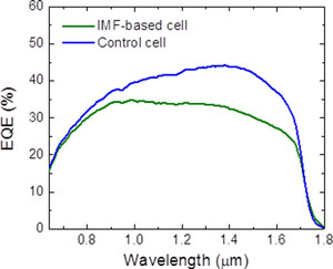
The response to AM1.5 solar illumination was reported for 400μm devices .The poorer performance of the GaAs-based cell is thought to be due to 60° threading dislocations. The spectral behavior of the external quantum efficiency (EQE) was also measured (Figure 2). The fall-off at longer wavelengths for the GaAs-based device as the bandgap is approached, compared with the control cell, suggests an additional loss process for photons in this region due to an increased density of non-recombination centers near the IMF region.

Figure 2: External quantum efficiency curves of 400μm-diameter TPV cells.
The researchers comment: "Even though the majority of IMF arrays are 90° misfit dislocations confined at the interface, the randomly formed 60° misfit dislocations representing imperfect relaxation affect the epitaxial layers above. The longer-wavelength photons will travel deeper into the devices and be absorbed near the GaSb/GaAs interface."
The researchers hope that further work to optimize the IMF growth technique and to reduce carrier recombination near the GaSb/GaAs interface will improve cell performance. "However, it is encouraging that the difference in EQE spectra between the control and IMF-based cells is within 10% over the entire range of wavelengths studied," the team adds.


