A team of engineers from Cornell University, the University of Notre Dame and the semiconductor company IQE has created gallium nitride (GaN) power diodes capable of serving as the building blocks for future GaN power switches -- with applications spanning nearly all electronics products and electricity distribution infrastructures.
Power semiconductor devices are a critical part of the energy infrastructure -- all electronics rely on them to control or convert electrical energy. Silicon-based semiconductors are rapidly approaching their performance limits within electronics, so materials such as GaN are being explored as potential replacements that may render silicon switches obsolete.
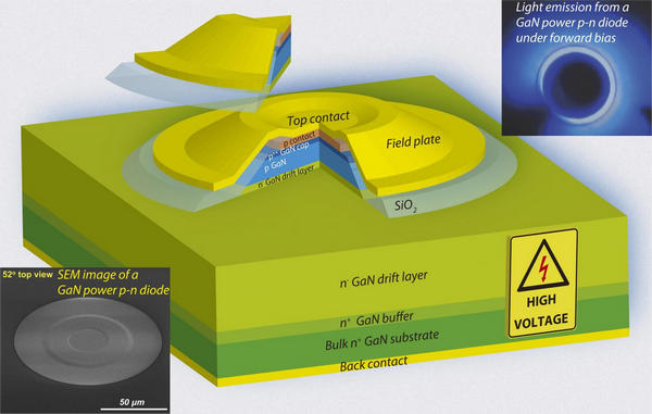
This image shows a state-of-the-art design of GaN p-n junction diodes that has resulted in near-unity ideality factor, avalanche breakdown capability, and record-breaking power performance. Insets show a GaN p-n diode fabricated on a high-quality bulk GaN substrate and light emission from the junction under forward bias. (Photo courtesy of Zongyang Hu)
But along with having many desirable features as a material, GaN is notorious for its defects and reliability issues. So the team zeroed in on devices based on GaN with record-low defect concentrations to probe GaN's ultimate performance limits for power electronics. They describe their results in a paper in the journal Applied Physics Letters, from AIP Publishing.
"Our engineering goal is to develop inexpensive, reliable, high-efficiency switches to condition electricity -- from where it's generated to where it's consumed within electric power systems -- to replace generations-old, bulky, and inefficient technologies," said Zongyang Hu, a postdoc working in Professor Grace Huili Xing's research group within the School of Electrical and Computer Engineering at Cornell University. "GaN-based power devices are enabling technologies to achieve this goal."
The team examined semiconductor p-n junctions, made by joining p-type (free holes) and n-type (free electrons) semiconductor materials, which have direct applications in solar cells, LEDs, rectifiers in circuits, and numerous variations in more complex devices such as power transistors. "For our work, high-voltage p-n junction diodes are used to probe the material properties of GaN," Hu explained.
To describe how much the device's current-voltage characteristics deviate from the ideal case in a defect-free semiconductor system, the team uses a "diode ideality factor." This is "an extremely sensitive indicator of the bulk defects, interface and surface defects, and resistance of the device," he added.
Defects exist within all materials, but at varying levels. "So one parameter we used to effectively describe the defect level in a material is the Shockley-Read-Hall (SRH) recombination lifetime," Hu said.
SRH lifetime is the averaged time it takes injected electrons and holes in the junction to move around before recombining at defects. "The lower the defect level, the longer the SRH lifetime," Hu explained. "It's also interesting to note that for GaN, a longer SRH lifetime results in a brighter light emission produced by the diode."
The work is significant because many researchers around the globe are working to find ways to make GaN materials reliable for use within future electronics. Due to the presence of defects with high concentrations in typical GaN materials today, GaN-based devices often operate at a fraction of what GaN is truly capable of.
It's worth noting that, in 2014, a Nobel Prize in physics was awarded to three scientists for making seminal and breakthrough contributions to the field of GaN-based LEDs. Though operating at compromised conditions, GaN LEDs are helping to shift the global lighting industry to a much more energy-efficient, solid-state lighting era.
The work led by Xing at Cornell University is the first report of GaN p-n diodes with near-ideal performance in all aspects simultaneously: a unity ideality factor, avalanche breakdown voltage, and about a two-fold improvement in device figure-of-merits over previous records.
"Our results are an important step toward understanding the intrinsic properties and the true potential of GaN," Hu noted. "And these achievements are only possible in high-quality GaN device structures (an effort led by IQE engineers) prepared on high-quality GaN bulk substrates and with precisely tuned fabrication technologies (an effort led by Dr. Kazuki Nomoto, a research associate at Cornell University)."
One big surprise for the team came in the form of unexpectedly low differential-on-resistance of the GaN diode. "It's as if the body of the entire p-n diode is transparent to the current flow without resistance," he said. "We believe this is due to high-level injection of minority carriers and their long lifetime, and are exploring it further."
The team's work is part of the U.S. Department of Energy's (DOE) Advanced Research Projects Agency-Energy (ARPA-E) "SWITCHES" program, monitored by Dr. Timothy Heidel. "Leading one of these projects, we at Cornell, in collaboration with our industrial partners IQE, Qorvo, and UTRC, have established an integrated plan to develop three terminal GaN power transistors, package them, and insert them into circuits and products," Xing said.
Beyond the DOE ARPA-E project, the team is open to collaboration with any researchers or companies interested in helping drive GaN power electronics to its fruition.
This image shows a state-of-the-art design of GaN p-n junction diodes that has resulted in near-unity ideality factor, avalanche breakdown capability, and record-breaking power performance. Insets show a GaN p-n diode fabricated on a high-quality bulk GaN substrate and light emission from the junction under forward bias.


