University of Notre Dame (UND) in the USA and epiwafer maker IQE have claimed record-breaking balanced frequency performance for a nitride semiconductor high-electron-mobility transistor (HEMT) using indium aluminium gallium nitride (InAlGaN) barriers [Ronghua Wang et al, IEEE Electron Device Letters, published online 23 January 2013].
Nitride HEMTs with rectangular gates can have high-performance current-gain cut-offs (fT), while power-gain cut-off frequencies (fmax) are enhanced by using T-shaped gate profiles. Ideally the two cut-off frequency characteristics should be close to one another for best performance. Using a rectangular gate reduces parasitic capacitance; T-gates are more conductive.
The UND/IQE devices used InAlGaN barriers to enhance the channel mobility, allowing a T-gate to be used. The epitaxial structure (Figure 1) was grown on silicon carbide (SiC) using metal-organic chemical vapor deposition (MOCVD). The ohmic contact metal electrodes consisted of titanium/gold on 140nm-thick n-GaN source-drain regions re-grown using molecular beam epitaxy (MBE). The source-drain distance was 0.8μm.
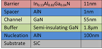
Figure 1: Epitaxial structure of HEMTs.
T-gates were produced that consisted of nickel/gold. There was no passivation. The width of the T-gate was 2μm x 2μm. The stem height was ~100nm. The head of the T was 350-400nm and the foot was 40-100nm.
Hall measurements gave the epitaxial material a sheet resistance of 195Ω/square, a carrier density of 1.8x10¹³/cm2, and mobility of 1770cm2/V-s.
The maximum drain current for a 40nm gate device was 1.8A/mm at 1V gate potential. The peak extrinsic transconductance of the same device was 770mS/mm. The current-gain (fT) and power-gain (fmax) cut-off frequencies (Figure 2a) were 230GHz and 300GHz, respectively (133/260GHz before de-embedding). The drain bias for the transconductance and frequency measurements was 5.6V.
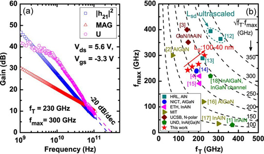
Figure 2: (a) Small-signal RF performance of a 40nm-long HEMT showing fT/fmax = 230/300 GHz. (b) Comparison of fT and fmax of UND/IQE devices with state-of-the-art depletion-mode (normally-on) GaN-based HEMTs from research literature. The ‘Lsd ultrascaled’ devices (2011) included back-barriers.
The geometric mean of fT and fmax (square root of product) was 263GHz. The balanced frequency performance is claimed as a record for devices with InAlGaN barriers (with no back-barrier). The researchers reference as the previous best a 30nm-gate device with InAlN barrier that achieved fT/fmax of 205/220GHz, reported in 2011 by Switzerland’s ETH Zurich. They also compare their device with a range of other reports from the research literature (Figure 2b).
The UND/IQE devices did show larger extrinsic parasitic delay effects due to the capacitance arising from the T-head of the gate compared with rectangular gates. The researchers believe this effect can be reduced by lengthening the T-stem to more than 200nm. Also, gate recessing would be beneficial in increasing transconductance.
The researchers add: “Furthermore, incorporation of re-grown contacts with a lower contact resistance and use of shorter gate lengths in conjunction with back-barriers (provided this is done without compromising the channel mobility) promise fT/fmax near 350GHz.”
This work was financially supported by the US Defense Advanced Research Projects Agency’s Nitride Electronic NeXt-Generation Technology program, the US Air Force Office of Scientific Research, and the US Air Force Research Laboratory/Missile Defense Agency.