South Korea's Hongik University has developed a nitride semiconductor device on silicon with an embedded Schottky barrier diode (SBD) [Bong-Ryeol Park et al, Appl. Phys. Express, vol6, p031001, 2013].
The device was designed as a normally-off switching transistor in forward operation and as a diode in reverse operation. One such component was able to withstand voltages up to 966V before breakdown. The research team suggests that two such switching devices could be used to implement a single-phase half-bridge DC–AC inverter circuit. Other possible applications include DC–DC energy conversion.
"The proposed device is very promising for use in high-efficiency monolithic converter and inverter ICs; eliminating the external diode can dramatically reduce the chip size, minimizing the parasitic inductance and thus allowing fast switching operation," they write.
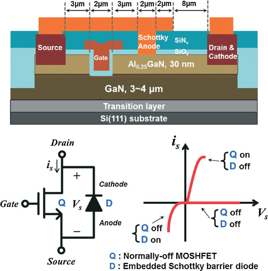
The epitaxial structure was created on p-type (111) silicon (Figure 1). The devices were isolated using low-damage mesa inductively coupled plasma (ICP) reactive ion etch. Normally-off operation of the transistor was achieved by etching through the aluminium gallium nitride (Al0.25Ga0.75N) barrier. The etched structure was covered by 30nm of silicon dioxide (SiO2) insulation using ICP chemical vapor deposition (CVD). The ohmic source-drain metals were silicon/titanium/aluminium/molybdenum/gold annealed at 850°C for 30 seconds. The gate and pad regions were nickel gold.

Figure 1: Cross-sectional schematic, equivalent circuit, and current–voltage (I–V) characteristics of SBD-embedded AlGaN/GaN-on-Si power switching device.
A further 180nm insulation layer of silicon nitride (SiNx) was applied. The Schottky anode and cathode regions of the embedded diode were then ICP reactive-ion etched into the SiNx. The anode was electrically connected to the source terminal of the transistor. The cathode was overlayed on top of the drain terminal. The metallization for the embedded diode consisted of nickel/gold.
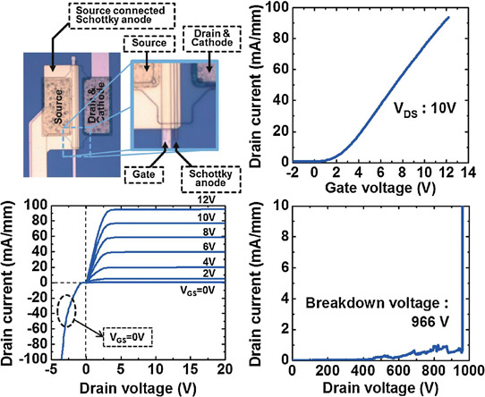
The transistor turned on at 2V with an on-resistance of 5.2mΩ-cm2. The 1mA/mm forward turn-on voltage of the Schottky barrier diode was 0.8V. A device with 10μm anode-cathode distance had off-state (0V gate) breakdown at 966V (Figure 2).

Figure 2: (a) Microscopy image of fabricated device, (b) transfer and (c) forward and reverse I–V, and (d) off-state breakdown characteristics of a fabricated device.
The researchers see an advantage of their device as being the ability to independently adjust the turn-on voltages of the transistor and diode. The transistor turn-on is affected by the recess depth and the gate insulator thickness. The diode turn-on is determined by the Schottky metal structure. This variability could allow optimization of the epitaxial design and device structure to improve performance characteristics.


