Epistar hints at'game-changing'silicon LED switch 12 Oct 2012 Giant Taiwanese LED maker works with GaN-on-silicon specialist Azzurro on technology with potential to cut cost of solid-state lighting.

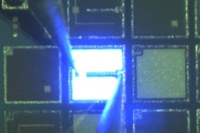
Plessey's GaN-on-silicon LED
Epistar,the Taiwan-based company that is ranked as one of the world's largest manufacturers of high-brightness LEDs,has become the latest major producer to hint at a transfer to a potentially much cheaper silicon platform.
Currently the vast majority of blue LEDs,including Epistar's,are made by depositing light-emitting layers of gallium nitride and related semiconductor material on top of a sapphire substrate.But the use of sapphire represents a significant proportion of the eventual cost of the LED,and a switch to silicon wafers could according to its proponents-cut the cost of chips used in solid-state lighting by as much as 80%.
If high performance and reliability can be achieved in mass production,using legacy silicon CMOS processing lines,that would no doubt accelerate the move away from inefficient incandescent lighting to its far less energy-intensive semiconductor replacement.
The problem is that silicon and gallium nitride crystals have a serious lattice mismatch at the atomic level,and require a so-called"strain engineering"approach to wafer fabrication to ensure that the LEDs produced function properly,stopping wafers from bowing and cracking under the high temperatures required in key LED processing steps.
That requires the deposition of extra layers of material to act as a buffer between the two mismatched lattices,adding to the processing time and reducing the cost advantage of the technology.
Game-changera
Now Germany's Azzurro Semiconductors,a specialist in the GaN-on-silicon wafer technology,says that Epistar has been able to transfer its existing LED layer structures to 150 mm diameter silicon wafers after a development period of only 16 weeks.Azzurro's strain-engineered templates allow customers to transfer their own proprietary LED structures onto the new format without major process changes.
The company's approach,detailed in this white paper,is to deposit a thick n-GaN buffer layer to compensate for the lattice mismatch.According to Erwin Ysewijn,Azzurro's VP of marketing and sales,despite the thickness of the buffer,the overall growth time needed to deposit the LED layer structure works out to be the same for both silicon and sapphire production.
Ysewijn would not say whether or not Epistar was now planning to transfer the technology into mass production,although the Taiwan company's chairman hinted that this could happen in a statement issued by the German firm:
We are very excited about the outcome of this joint exercise,which has exceeded all expectations regarding speed and cost of migration,said Lee Biing Jye.The success helps us to utilize GaNon silicon,which is a game changer for the industry and Epistar as a leading innovator is part of it.
Potentially disruptive
Epistar is by no means the first company to work on the potentially disruptive technology.Osram Opto Semiconductors has been collaborating with Azzurro for a number of years,and announced very promising results from its laboratory earlier this year.Ysewijn told optics.org that Osram was strongly committed to GaN-on-silicon technology,and that Azzurro was working with a number of other leading companies.
As well as the leading chip makers,a number of start-up firms are also trying to enter the market with their own proprietary versions of GaN-on-silicon LEDs.They include China's Lattice Power,US-based Bridgelux(now working closely with investor Toshiba)and the UK company Plessey Semiconductors,which is aiming to transfer technology initially developed at Cambridge University to its production facility.
To truly take advantage of legacy silicon infrastructure,a much more convincing economic argument for the GaN-on-silicon approach can be made with 200 mm wafers.Ysewijn told optics.org that while GaN-on-silicon made sense at 150 mm wafer sizes,the larger format would make the case even more strongly.
Azzurro is already working on that larger format with the help of a 2.6 million grant awarded in July 2012 and financed via the European Regional Development Fund and the Free State of Saxony.
Erwin Wolf,the Azzurro CEO,said:The technology to enable the LED industry to tap into the advantages of the volume,cost-effectiveness and maturity of silicon foundries is ready with our strain engineered templates.


