Led by the Department of Energy's Oak Ridge National Laboratory (ORNL), a group of researchers has synthesized a stack of atomically thin monolayers of two lattice-mismatched semiconductors (Xufan Li et al, 'Two-dimensional GaSe/MoSe2 misfit bilayer heterojunctions by van der Waals epitaxy', Science Advances, Vol. 2, no. 4, e1501882). ORNL's Functional Hybrid Nanomaterials group, led by David Geohegan, conducted the study with partners at Vanderbilt University, the University of Utah, and Beijing Computational Science Research Center.
Stacking different materials on top of each other usually only works when the individual materials have very similar crystal lattices with a good lattice match. In contrast, the researchers have grown high-quality layers of very different two-dimensional (2D) materials, broadening the number of materials that can be combined and thus creating a wider range of potential atomically thin electronic devices.
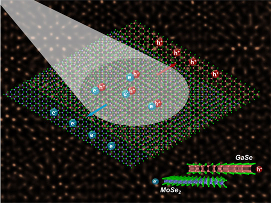
In the research, the interface between the two layers of p-type semiconductor gallium selenide (rich in hole charge carriers) and n-type semiconductor molybdenum diselenide (rich in electron charge carriers) formed an atomically sharp p–n junction heterostructure which generated a photovoltaic response by separating electron–hole pairs generated by light. "Because the two layers had such a large lattice mismatch between them, it's very unexpected that they would grow on each other in an orderly way," says ORNL's Xufan Li, lead author of the study. "But it worked." This atomically thin solar cell shows the promise of synthesizing mismatched layers to enable new families of functional 2D materials, say the researchers.
In particular, the group is first to show that monolayers of two different types of metal chalcogenides (binary compounds of sulfur, selenium or tellurium with a more electropositive element or radical) having such different lattice constants can be grown together to form a perfectly aligned stacking bilayer. "It's a new, potential building block for energy-efficient optoelectronics," Li said.

Picture: Light drives the migration of charge carriers at the juncture between semiconductors with mismatched crystal lattices. The schematic's background is a scanning transmission electron microscope image showing the bilayer in atomic-scale resolution. Credit: Oak Ridge National Laboratory, US Dept. of Energy. Image by Xufan Li and Chris Rouleau.
Li first grew a monolayer of molybdenum diselenide, and then grew a layer of gallium selenide on top. This technique of 'van der Waals epitaxy' is named for the weak attractive forces that hold dissimilar layers together. "With van der Waals epitaxy, despite big lattice mismatches, you can still grow another layer on the first," Li says. Using scanning transmission electron microscopy, the team characterized the atomic structure of the materials and revealed the formation of Moiré patterns.
Upon characterizing their new bilayer building block, the researchers found that the two mismatched layers had self-assembled into a repeating long-range atomic order that could be directly visualized by the Moiré patterns they showed in the electron microscope. "We were surprised that these patterns aligned perfectly," Li says.
"These new 2D mismatched layered heterostructures open the door to novel building blocks for optoelectronic applications," says senior author Kai Xiao of ORNL. "They can allow us to study new physics properties which cannot be discovered with other 2D heterostructures with matched lattices," he adds. "They offer potential for a wide range of physical phenomena ranging from interfacial magnetism, superconductivity and Hofstadter's butterfly effect."
The researchers plan future studies to explore how the material aligns during the growth process and how material composition influences properties beyond the photovoltaic response. The research advances efforts to incorporate 2D materials into devices. "We've opened the door to exploring all types of mismatched heterostructures," says Li.
The research, including materials synthesis, was supported by the DOE Office of Science. Materials characterization was conducted in part at the Center for Nanophase Materials Sciences (a DOE Office of Science User Facility at ORNL). ORNL Laboratory Directed Research and Development funds supported some of the device measurements in the study.