Researchers in Japan and USA have claimed the first experimental demonstration of higher breakdown voltage for slant field-plate (FP) gallium nitride (GaN) high-electron-mobility transistors (HEMTs) over convention field-plate designs [Kengo Kobayashi, et al, Appl. Phys. Express, vol7, p096501, 2014].
Field plates are used in GaN HEMTs to manipulate and reduce peak electric fields, allowing higher voltages to be achieved. Generally, field plates consist of layers of metal on insulating dielectric parallel to the underlying semiconductor materials. Higher voltage performance can be achieved with multiple layers of FPs and dielectric, but with increased complexity and cost.
Inspired by numerical simulations from a few years ago suggesting better breakdown performance, the team at Tohoku University and Massachusetts Institute of Technology (MIT) set out to create slant field plates on GaN HEMT structures. Metal-organic chemical vapor phase epitaxy was used to create semiconductor heterostructures with a gallium nitride buffer, aluminium nitride (AlN) spacer, and aluminium gallium nitride (AlGaN) barrier on semi-insulating sapphire.
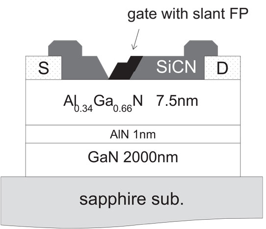
The HEMT fabrication (Figure 1) consisted of titanium/aluminium/titanium/platinum/gold ohmic metal deposition, mesa isolation plasma etch, 780°C ohmic annealing, plasma-enhanced chemical vapor deposition (PECVD) of silicon carbon nitride (SiCN) surface passivation, gate and field-plate formation, and ohmic contact access etch and deposition of titanium/platinum/gold source/drain electrodes.

Figure 1: Cross-sectional view of AlGaN/GaN HEMT with slant field plate.
The test devices had a gate length of 230nm with gate separations from the source and drain of 4μm each.
The SiCN PECVD used hexamethyldisilazane (HMDS) vapor to create a 200nm film. The carrier gases were hydrogen and ammonia. The gas-balance allowed variation of the SiCN composition, resulting in different plasma-etch characteristics. SiCN produced with ammonia carrier is more easily etched, compared with SiCN from hydrogen carrier.
Variation of the carrier from pure hydrogen to pure ammonia in ten steps allowed the researchers to create a slant surface for the field plate when the gate window was created with plasma etching. The etch was carried out in two parts: first a vertical reactive-ion etch with carbon hexafluoride (C2F6), followed by a lateral etch with sulfur hexafluoride (SF6).
The gate metals were nickel/gold. The field-plate metal was evaporated onto the sample, which was tilted to ensure that the metal was deposited on the drain side slant of the SiCN passivation. Devices were also produced where the SiCN layer was produced in 3- and 4-steps, giving field plates with different characteristics. Having 10 steps gives a practically smooth slanted FP.
The DC characteristics of the three test devices were almost identical. In the off-state, the bulk of the drain current comes from gate leakage. All the devices were able to sustain voltage sweeps to 160V without hard breakdown. By contrast, a comparison device without a field plate suffered hard breakdown at 83V.
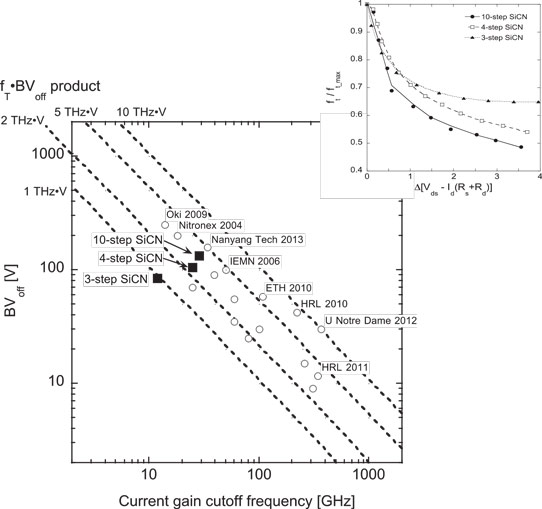
The off-state breakdown (BVoff) increased with the number of steps used in depositing the SiCN passivation. Defining the breakdown voltage as that giving a drain current of 1mA/mm, the researchers found the 10-step device to have 66% greater BVoff over a HEMT with a conventional double field-plate design.
The frequency performance was also measured. The maximum current-gain cut-off frequencies (fT) were 12GHz, 24.7GHz, and 28.8GHz for 3-, 4-, and 10-step field plates. The HEMT without a field plate also had an fT of 12GHz, like the 3-step HEMT. However, the maximum current density was halved in the device without field plate.

Figure 2: BVoff versus fT for various GaN-based HEMTs, including Tohoku/MIT devices. Inset: change in fT normalized with respect to maximum value (fT/fT_max) as effective drain voltage, Vds – Id(Rs + Rd), increases from value for fT_max.
Although the 10-step HEMT has the best frequency performance, the fT decreases more rapidly with increased drain bias in comparison with the other devices. The maximum fT and BVoff values give a 4-fold advantage for the BVoff.fT product of the 10-step device over HEMTs with conventional field plates (Figure 2).


