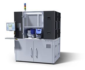
EV Group (EVG) of St Florian, Austria, a supplier of wafer bonding and lithography equipment, has introduced the latest version of its EVG120 automated resist processing system. Incorporating new features and improved productivity in an ultra-small footprint design, the system supports coating and developing applications for a variety of markets, including compound semiconductors, microelectromechanical systems (MEMS), and advanced packaging. The tool can be configured with combined spin and spray coating modules—a unique feature that maximizes productivity and optimizes cost of ownership, says the firm.

Picture: EVG120 automated resist processing system.
Dr. Thomas Glinsner, head of product management for EV Group, said, "Our new EVG120 system reflects EVG's 15 years of experience in resist coating and developing, and our unique process skills. In independent surveys, our customers consistently attribute the highest scores to EVG's lithography equipment, and we've listened to their feedback to create a more optimized system. Based on a proven platform, the next-generation EVG120 coater/developer offers increased functionality and reliability in a highly customizable and economical package."
The EVG120 automated resist processing system features a new robot with dual arms for fast wafer swapping and additional processing chambers, which result in enhanced throughput and overall productivity. To further optimize throughput and overall productivity, the system runs the same EVG CIM Framework software as EVG's high-end XT Frame systems and offers full software integration with SECS/GEM standards. Two customizable wet processing bowls are complemented by 10 stacked modules for vapor prime, soft and hard bake, and chill processes. EVG120 can accommodate wafers up to 200 mm in diameter.
Other new features of the system include EVG's CoverSpin rotating bowl cover that allows improved coating uniformity across the substrate regardless of substrate shape. A new, temperature-controlled chuck further enhances EVG's proprietary OmniSpray coating technology, which specifically allows conformal coating of high-topography surfaces via its proprietary ultrasonic nozzle. OmniSpray coating is suited for ultra-thin, fragile or perforated wafers and can result in an 80% or greater reduction in material consumption compared to traditional spin coating, adds the firm.
EVG120 is suited for a wide variety of markets and applications, including: high-topography coating and spray coating for MEMS; thick-film resists and bumping for advanced packaging; and passivation, dielectrics and thick-film processing for compound semiconductor devices.