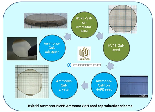
Ammono S.A. in Warsaw, Poland, which produces bulk gallium nitride (GaN) using ammonothermal technology, and the Institute of High Pressure Physics of the Polish Academy of Sciences (Unipress) say they have conceived proprietary new technology that allows cheap and fast production of ammonothermal GaN on the basis of hybrid Ammono-HVPE GaN seeds.
Ammonothermal gallium nitride is seen as a perfect material for performance-driven electronic and optoelectronic applications, which require very good crystal quality, says Ammono. An example is the laser diode, where output power and lifetime depend strongly on GaN substrate quality. Other examples are power transistors and Schottky diodes, where reliability is related primarily to the device’s crystalline structure and thus substrate quality. Last but not least, ultra-high-brightness LEDs benefit tremendously from the substrate’s low dislocation density, which allows effective dissipation of the heat created during device operation.
Competing GaN production technologies such as hydride vapour phase epitaxy (HVPE) or liquid phase epitaxy (LPE) use foreign (non-GaN) seeds, and the quality of the GaN material obtained in this way results in the manufacture of devices that, on a long-term scale, do not achieve the quality targets set by device makers, claims Ammono. This lower quality is reflected in many parameters, most importantly the dislocation density, which in the case of ammonthermal GaN is of the order of 104cm-2 whereas other technologies are at least two orders of magnitude worse, adds the firm.
Ammono and Unipress have shown that using hybrid HVPE-ammonthermal approaches allows the manufacture of GaN material fulfilling the strict requirements of high-end applications. In the framework of a grant received from the Polish National Center for Research and Development (PBS1/B5/7/2012) it was shown that, by using ammonothermally grown GaN (as a seed), one can obtain high-quality free-standing HVPE-GaN (for details, see Appl. Phys. Expri 6, 075504 (2013)).
Smooth GaN layers up to 2.5mm thick (crystallized with a stable growth rate of 240μm.hr-1) and of an excellent crystalline quality, without cracks, and with low threading dislocation density (5x104 cm-2) have been grown and then sliced from the Ammono-GaN seed wafers (see Figure).

The structural properties of the free-standing HVPE-GaN do not differ from the structural properties of the Ammono-GaN seeds, notes the firm. Additionally, this is a high-purity material. According to the SIMS analysis the oxygen and carbon content is below 1016cm-3. The only silicon impurity is of the order of 3x1016cm-3.
Thus, from the point of view of physical properties, the HVPE-GaN is of a much higher quality than the that obtained using MOCVD-GaN/sapphire templates or GaAs crystals as seeds, it is claimed.
Subsequently, the new material was used again as a seed for the ammonthermal process. As a result, a new kind of GaN crystal was grown (Ammono-HVPE-Ammono). Their characteristics were presented for the first time during the Gallium Nitride Materials and Devices IX conference at SPIE’s Photonics West 2014 event in San Francisco. A threading dislocation density of 2x105cm-2 and average full width at half maximum (FWHM) of 19 arcsec define the new ammonothermal material as top class compared with other existing GaN manufacturing approaches, claims Ammono.
The new proprietary and patent protected technology allows high-volume, high-quality GaN seed replication, which will accelerate the spread of ammonthermal GaN to mass-market applications, the firm reckons. It will also allow Ammono-GaN production costs to be driven down in an aggressive way due to much faster availability of a vast population of high-quality GaN seeds, it concludes.


