Researchers in the USA have been working on gallium nitride phosphide (GaNP) as an absorbing material for solar power [S. Sukrittanon et al, Appl. Phys. Lett., vol107, p153901, 2015]. The aim of the team from University of California San Diego (UCSD) and Sandia National Laboratories is to create a suitable sub-cell to boost the performance of silicon-based photovoltaic power conversion. Theory suggests that conversion efficiencies up to 45% could be achieved from an AM1.5G solar spectrum with a III-V material on silicon.
Gallium phosphide is one contender for such a top cell since it is near lattice matched (0.37% mismatch) and has a suitable bandgap of 2.26eV. Unfortunately GaP has an indirect bandgap, which makes for inefficient photon conversion to electric power.
With the addition of only 0.4% of nitrogen into GaP, giving GaNP, the bandgap becomes direct, shifting absorption coefficients from 102-103/cm towards 104/cm. Further, at a nitrogen concentration of 2%, GaNP becomes lattice matched with silicon.
The UCSD/Sandia researchers achieved efficiencies up to 7.9% without a window layer. The team comments: "This GaNP solar cell's efficiency is 3x higher than the most efficient GaP solar cell to date and higher than other solar cells with similar direct bandgap (InGaP, GaAsP)." They add: "These performance gains are expected to motivate further investigation into the integration of GaNP into future dual-junction solar cells on Si substrate."
The solar cells were grown on GaP substrates by molecular beam epitaxy (MBE) at 570°C (Figure 1). The GaNP bandgap was ~2.05eV, with the lattice almost matched to silicon. The mismatch from GaP was 0.31%. The nitrogen concentration was around 1.8%, according to x-ray analysis. In fact, GaP has a closer lattice match to silicon than any other III-V semiconductor, note the researchers.
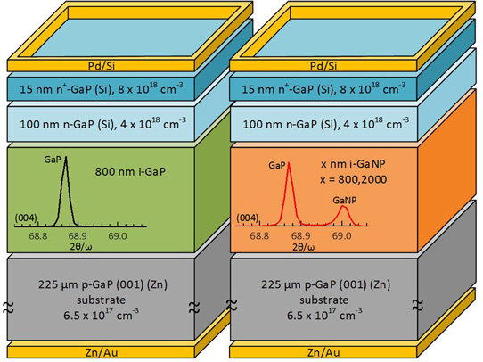
Figure 1: Cross-sections of GaP control and GaNP solar cells. Inset: x-ray diffraction (XRD) spectra.
The n-type layers were designed to act as an emitter layer and a more heavily doped layer to reduce series resistance with the metal contact. The devices did not include a window layer. A control solar cell with GaP absorbing layer was also produced.
The GaNP samples were annealed in nitrogen/hydrogen forming gas at 750° for 30 seconds to suppress defects from nitrogen incorporation, low growth temperature, and RF nitrogen plasma damage.
The material was fabricated into 1mmx1mm solar cells. Further annealing was performed to improve the ohmic contact of the metal layers. An anti-reflective (AR) coating of silicon nitride and silicon dioxide layers was applied to some of the devices.
The current-voltage characteristics were measure in dark and AM1.5G solar condition. The GaNP cell showed a higher ideality (n) factor of more than 2, compared with 1.8 for the GaP cell. This indicated that the GaNP cell suffered from higher Shockley-Read-Hall recombination, reducing efficiency. This was likely caused by defects at GaP/GaNP interfaces.
Table 1: Performance parameters of GaP-800, GaNP-800, and GaNP-2000 with and without AR coating.
| Sample | Jsc (mA/cm2) | Voc (V) | Jsc-ratio (%) | FF (%) | η (%) | n-factor |
| Without AR | ||||||
| GaP-800 | 2.69 | 1.19 | 30 | 77 | 2.5 | 1.8 |
| GaNP-800 | 5.52 | 1.26 | 42 | 73 | 5.1 | 2.7 |
| GaNP-2000 | 7.80 | 1.31 | 60 | 71 | 7.3 | 2.0 |
| With AR | ||||||
| GaP-800 | 3.17 | 1.19 | 35 | 76 | 2.9 | … |
| GaNP-800 | 6.08 | 1.26 | 46 | 71 | 5.5 | … |
| GaNP-2000 | 8.53 | 1.33 | 65 | 69 | 7.9 | … |
Sample Jsc (mA/cm2) Voc (V) Jsc-ratio (%) FF (%) η (%) n-factor Without AR GaP-800 2.69 1.19 30 77 2.5 1.8 GaNP-800 5.52 1.26 42 73 5.1 2.7 GaNP-2000 7.80 1.31 60 71 7.3 2.0 With AR GaP-800 3.17 1.19 35 76 2.9 … GaNP-800 6.08 1.26 46 71 5.5 … GaNP-2000 8.53 1.33 65 69 7.9 …
The performance was extracted from the current-voltage behavior (Table 1). Since GaP and GaNP respond to somewhat different wavelengths of the solar spectrum, the ratio of the current density compared with the maximum possible (i.e. for external quantum efficiency of 1) was determined to give a fairer comparison.
The fill factor (FF) of the GaNP devices was slightly lower than for the GaP device, but this was compensated by higher open-circuit voltage (Voc) and short-circuit current density (Jsc). (FF = maximum obtainable power/(VocxJsc).)
With a thicker 2000nm GaNP layer, both Voc and Jsc increased due to the greater light absorption length. The researchers comment: "Our work shows that efficiency is not yet limited by minority carrier diffusion length. Thus, this trend may continue beyond the maximum thickness, 2000nm in GaNP-2000, studied in this work."
Anti-reflective coatings increased Jsc but had little effect on Voc. The best cell with anti-reflective coating and 2000nm GaNP absorbing layer had an efficiency (η) of 7.9%.
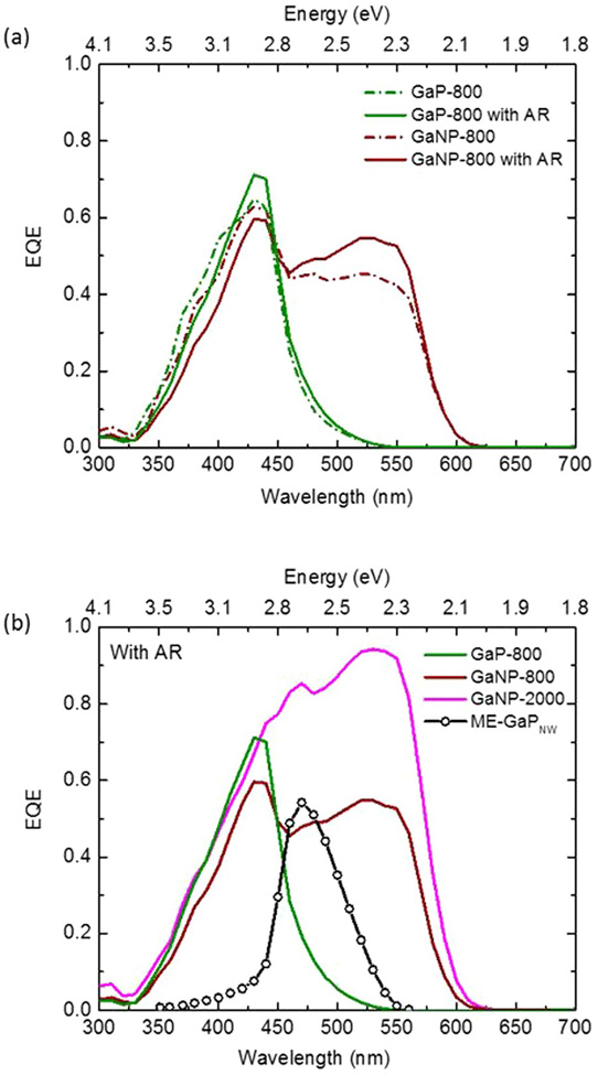
Figure 2: (a) EQE measurements with and without an AR coating of GaP-800 and GaNP-800. (b) EQE measurements with an AR coating of GaP-800, GaNP-800, GaNP-2000, and ME-GaPNW, a device from another group with 2.42% efficiency (without window layer), reported 2012.
External quantum efficiency (EQE) spectra suggested that the anti-reflective coatings reduced efficiency at shorter wavelengths (Figure 2). This was attributed to absorption by silicon nitride, which has a bandgap in the region 2.4-4.7eV. The researchers believe that improvements in EQE can be achieved through "(1) increasing the diffusion length in the emitter region (e.g. optimizing growth conditions), (2) optimizing the emitter thickness, and (3) reducing the front surface recombination velocity (e.g. passivating the front surface, implementing a window layer)."
According to the researchers, the current best solar efficiency for GaP devices is 2.9% with a window layer and 2.4% without. These devices had a thicker absorbing layer than the 800nm of the GaP control device, which benefited from an emitter layer that was thinner than the hole diffusion length.
The researchers conclude: "To date, our GaNP solar cells exhibit higher efficiency than other wide-bandgap solar cells grown on GaP substrate. InGaP (2.12eV) and GaAsP (1.92eV) solar cells with active layer thicknesses of 2μm achieve efficiencies of only 3.89% and 4.8%, respectively; the low efficiencies partly result from their lattice mismatch, which requires the growth of defective metamorphic buffer layers."


