University of California Santa Barbara (UCSB) in the USA has developed a monolithic white light-emitting diode (LED) with blue light produced by electrical pumping, and green/'red' by optical pumping from the blue source [S. J. Kowsz et al, J. Appl. Phys., vol120, p033102, 2016]. Also, the polarization properties of the device could be useful for more efficient liquid-crystal display (LCD) back lighting.
Normally, white LEDs consist of electrically pumped blue or ultraviolet light that pumps a broad-band yellow phosphor. The UCSB semi-polar device added green and 'red' indium gallium nitride (InGaN) quantum wells to those for the blue LED. The 'red' section of the device used doping-profile band engineering to shift to longer wavelengths with a relatively small increase in indium content to narrow the bandgap.
By using optical pumping for the long-wavelength emissions, the devices avoid the problems of electrical transport through high-indium-content InGaN caused by lower material quality. Also, the carrier densities in optically pumped quantum wells (QWs) are lower, which reduces non-radiative efficiency-sapping Auger-like recombination. Also, lower carrier density means lower screening of the red-shift effects of the band engineering, which would reduce the wavelength in the blue direction.
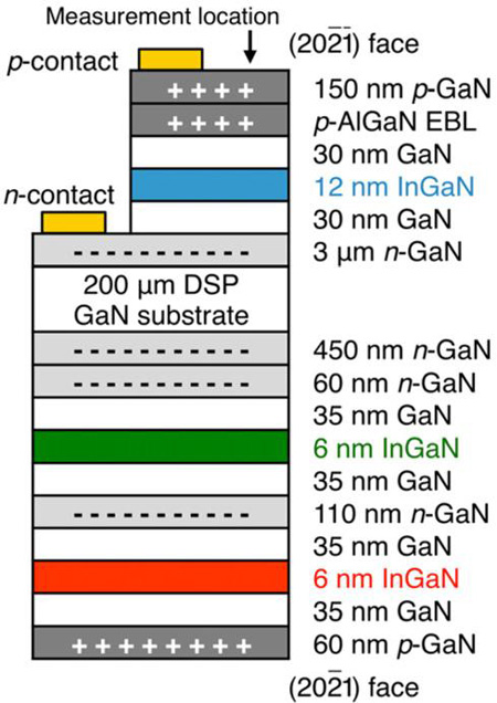
The blue LED component was grown first by metal-organic chemical vapor deposition (MOCVD) on the (20-2-1) face of a 7.5mmx7.5mm bulk GaN substrate from Mitsubishi Chemical (Figure 1). The researchers comment: "Previous work has demonstrated that blue LEDs with high power, low electrical droop, and small wavelength shift can be grown on this plane."

Figure 1: Cross-sectional schematic of epitaxial structure of UCSB white light-emitting semi-polar device.
The optically pumped material was grown on the (20-21) side of the substrate. By growing this material after the high-temperature blue LED process, the researchers avoided degradation of the higher-indium-content InGaN needed for longer-wavelength emission. Also, high-indium-content InGaN grown on (20-21) planes suffers less from stacking faults, compared with (20-2-1) deposition. The (20-2-1)/(20-21) planes also allow devices that produce polarized light.
Another advantage of (20-21) growth for the optically pumped high-In-content InGaN is that a doping profile can be used to create a built-in electric field that augments polarization-induced electric fields, red-shifting the photoluminescence. In particular, the p-GaN must be grown last to allow acceptor activation by thermally driving out hydrogen from magnesium-hydrogen complexes that form with the magnesium doping.
The red shift means that the indium content does not need to be as high for a given wavelength. The higher-indium-content final p-i-n quantum well was grown at 10° lower temperature, compared with the shorter-wavelength n-i-n optically pumped quantum well.
The electrical contacts for the LED were fabricated with a circular palladium/silver/nickel/gold p-contact of 180μm radius, and scribing down to the n-GaN layer for a soldered indium n-contact.
The researchers simulated the optically pumped wells as In0.27Ga0.73N and In0.29Ga0.71N for the short and long wavelengths, respectively. "The change in the indium content for the different QWs corresponds to the different growth temperatures used in growing the optically pumped QWs in the experimental sample," the team comments.
The simulation suggests the red-shift for the long-wavelength QW from aligning the built-in and polarization-induced fields would be 76nm, compared with the short-wavelength QW. The band-engineering/doping component accounted for 57nm of the shift in simulation, and the higher indium content the remaining 19nm.
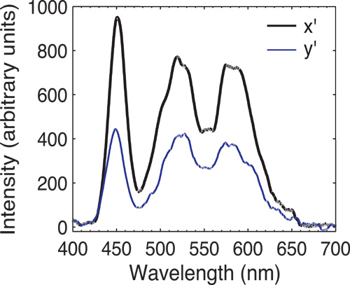
The spectral properties of the emission from the device varied according to the data collection position. At a distance of 680μm from the center of the p-contact, the emission consisted of a blue ~450nm peak from the LED with 10A/cm2 injection, a green ~520nm peak from the short-wavelength optically pumped QW, and a ~590nm 'red' peak from the long-wavelength QW (a 70nm red-shift). Although the device is billed as a RGB (red-green-blue) device by the researchers, 590nm is more strictly in the 590-620nm orange range. The balance of the components changed with position, with the longer wavelengths becoming more significant with distance from the p-contact.
The researchers compared the color rendering to that of more common blue-yellow (BY) devices often used to create 'white' light. "By producing light that is more widely distributed across the visible spectrum, the RGB device is able to render colors more faithfully than the BY device, which is important for general illumination. The RGB device would also be more energy efficient than the BY device for backlighting displays. Creating red, green and blue emission peaks would align the white light spectrum with the transmission spectra of display filters that are typically designed to transmit red, green and blue light, resulting in less light being lost to absorption in the filters."
The emission had 1931 Commission Internationale de l'Eclairage (CIE) x, y coordinates of (0.33, 0.35), a correlated color temperature (CCT) of 5604K, and a color rendering index (CRI) of 70. The optical polarization ratio for integrated intensities was 0.3 for polarization vectors aligned along [1-210] (x') and [10-1-4] (y') directions (Figure 2).

Figure 2: Electroluminescence spectra with polarizer aligned along x' and y' directions.
The polarization ratio was found to depend on measurement position, like the spectral properties. The researchers expect that the polarization ratio could be increased by improved color uniformity and extraction efficiency. In particular, the relative intensity of the longer wavelengths must be a focus of such work.
The team sees the need for developing growth conditions to increase the number, radiative efficiency and absorbance of optically pumped wells. The researchers comment: "Improved material quality and larger overlap of the electron and hole wavefunctions will result in better performance of the optically pumped QWs. In particular, because band engineering can enable the use of lower-indium-content InGaN or thinner QWs in achieving a desired emission wavelength, ongoing work is investigating the larger design space that is enabled by band engineering."


