Arizona State University (ASU) in the USA claims the first demonstration of 1kV-class aluminium nitride (AlN) Schottky barrier diodes (SBDs) [Houqiang Fu et al, IEEE Electron Device Letters, 5 July 2017].
AlN has a wide bandgap of 6.2eV. Wide bandgaps are associated with the large critical fields (12.5MV/cm in AlN), which are needed in compact power handling devices. Other semiconductor materials used in or proposed for power devices have narrower bandgaps: 3.3eV for silicon carbide, 3.4eV for gallium nitride, 4.8eV for beta-gallium oxide, and 5.5eV for diamond. AlN also has a large thermal conductivity of 340W/mK, which is also an attractive feature for power applications.
AlN’s advantages have not led so far to commercial devices since there are material and fabrication challenges.
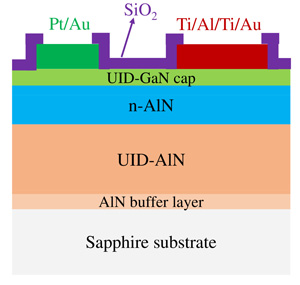
ASU’s AlN material was grown by metal-organic chemical vapor deposition (MOCVD) on single side-polished (0001) sapphire substrate off-cut 0.2°. The SBD structure (Figure 1) included 1μm unintentionally doped (UID) AlN underlayer (UL), 300nm silicon-doped n-AlN, and 2nm UID gallium nitride cap.
Figure 1: Schematic view of fabricated AlN Schottky barrier diodes on sapphire by MOCVD. Ohmic and Schottky contacts are in red and green, respectively.

According to the researchers, the device structure mimics silicon-on-insulator (SOI) technology, with a thin n-AlN epilayer active region on the thick resistive AlN underlayer. The purpose of the cap was to protect the underlying layers from oxidation, which can negatively impact device performance.
The researchers report that the AlN material demonstrated among the narrowest reported full-width at half maximum (FWHM) x-ray peaks for MOCVD AlN on sapphire – 46.8arcsec for the (0002) rocking curve and 159.1arcsec for (20-24). These figures suggest dislocation densities of the order 108/cm2.
The Schottky barrier diode was fabricated with 20nm/100nm/20nm/50 nm titanium/aluminium/titanium/gold (Ti/Al/Ti/Au) ohmic and 30nm/120nm platinum/gold (Pt/Au) Schottky contacts. The ohmic metal was patterned as a 400μm-diameter circular disk.
Two types of Schottky contact were made: a 100μm-diameter circular disk and 100μm-side square. The distance between the contacts was 200μm. Surface passivation consisted of 200nm plasma-enhanced CVD silicon dioxide (SiO2). There was no edge termination structure.
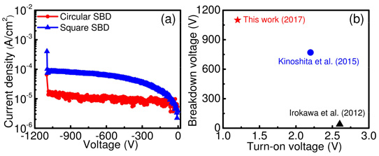
The ~105 on-off ratio of the devices is described by the team as being comparable to AlN devices on AlN substrates. The turn-on voltage of 1.2V (1.1V for square contacts) is smaller than previously reported values (more than 2V), according to ASU.
The temperature dependence of the device performance suggests that the forward current was limited by thermionic emission. The Schottky barrier height increased from 0.9eV to 1.6eV between 20°C (room temperature – RT) and 200°C. At the same time, the ideality decreased from 5.5 (5.3 for square contact) to 2.2. Previous reported idealities of AlN Schottky barrier diodes have been greater than 8.
The researchers attribute the ideality behavior to “lateral inhomogeneity of the Schottky barrier interface”. They add: “Note that the RT ideality factors (n = 5.5 and 5.3 for circular and square SBDs, respectively) obtained in this work were 2~3 times smaller than previous results, possibly due to improved material quality and metal/semiconductor interface.”
Figure 2: (a) Reverse current-voltage characteristics of circular and square AlN SBDs. (b) Comparison of breakdown and turn-on voltages of reported AlN SBDs.

Under reverse bias, the Schottky barrier diodes broke down only after 1kV, beating previous reports of ~700V for devices produced on free-standing AlN substrate by Japanese and US researchers (Figure 2). The ASU devices showed catastrophic damage at the edge of Schottky contacts that was attributed to edge electric field crowding.
The team comments: “Improvement in the breakdown capability of the devices can be further expected by employing field plate and/or edge termination. In addition, improving the material quality of n-AlN, increasing the resistivity of the UID AlN UL by Fe or C doping and optimizing the passivation strategies can also help to increase the breakdown voltage of the devices.”
Reverse bias leakage was generally less than 1nA.