k-Space Associates Inc of Dexter, MI, USA (which supplies thin-film metrology tools for the semiconductor, compound semiconductor and solar markets) has launched the kSA Emissometer. The ex-situ tool provides metal-organic chemical vapor deposition (MOCVD) fabs with essential wafer carrier characterization, including emissivity uniformity and defect identification.
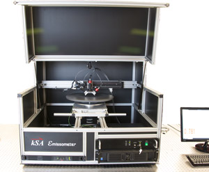
Picture: The new kSA Emissometer.
Traditionally, MOCVD fabs rely on subjective human tests to inspect the quality of wafer carriers after bakes and between runs, and then they rely on empirical data to adjust carrier temperatures from growth to growth, says k-Space. The kSA Emissometer is said to put the science back in carrier evaluation with high-resolution carrier emissivity mapping and the detection of defects and micro-cracks that are not visible to the human eye. The tool is designed to be used by operators and engineers and provides full quantitative carrier maps in 10 minutes.
"The real advantage of the kSA Emissometer is that it provides fabs with systematic carrier data that can be integrated into their quality control processes," says CEO Darryl Barlett. "It also provides a go-no-go decision on carrier use and quantitative determination of the carrier emissivity, allowing for temperature set-point adjustments for individual carriers," he adds. "In the end, this will lead to lower production costs and better device yields."


![[99.9% Alumina Ceramic Tube] 1600º C Heat Resistant 0.01mm Precision Custom Sizes Semiconductor/Gold Smelting Grade ISO 9001 Certified](https://image.made-in-china.com/3f2j00nWKeDOmMzJks/-99-9-Alumina-Ceramic-Tube-1600-ordm-C-Heat-Resistant-0-01mm-Precision-Custom-Sizes-Semiconductor-Gold-Smelting-Grade-ISO-9001-Certified.jpg "[99.9% Alumina Ceramic Tube] 1600º C Heat Resistant 0.01mm Precision Custom Sizes Semiconductor/Gold Smelting Grade ISO 9001 Certified")
