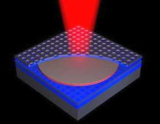
New surface-emitting laser design could improve speed and efficiency of optical connections.

On-chip laser,2 microns high
A new design of surface-emitting laser measuring just 2 microns in height could make it easier for manufacturers to integrate high-speed optical data connections into next-generation computers.The work has been published in Nature Photonics.
Developed by a team at the University of Texas at Arlington and the University of Wisconsin-Madison,the optically-pumped laser uses two highly reflective photonic crystal mirrors to replace the multiple layers of reflectors employed in the traditional distributed Bragg reflector laser design.
The resulting device,a membrane reflector VCSEL(MR-VCSEL),builds on the established principle that integrating silicon with a III–V gain medium is an attractive approach in the development of silicon lasers,because of its potential to yield high-efficiency sources.
The team used a combination of stamp-assisted transfer-printing and the stacking of semiconductor nanomembranes to create a InGaAsP quantum-well heterostructure able to act as the gain medium.This was sandwiched between two thin,single-layer silicon photonic-crystal reflectors,which were themselves fabricated via e-beam lithography and reactive ion etching.
"We apply a nanomembrane transfer printing process to accomplish this goal and integrate compound semiconductor quantum wells with silicon,"commented Weidong Zhou of UT Arlington,who explained that the technique is based on the use of a polydimethylsiloxane(PDMS)stamp.Similar PDMS transfer printing processes are already used to transfer various types of crystalline semiconductor materials onto foreign substrates and in soft lithography operations.Zhou noted that such a PDMS transfer printing method would be readily scalable to full wafer size.
According to Zhou and colleague Zhenqiang Ma from UW-Madison,one layer of photonic crystal in the new device is equal to about 15 to 30 layers of dielectric reflectors found in conventional lasers.As a result,manufacturers could fabricate 2-micrometer-high lasers for data links with performance able to equal that of current designs.
Shrinking sources
Edge-emitting lasers are promising contenders for on-chip optical links,but forming the necessary mirrors has proven to be difficult.Another issue is the sheer size of the source,since the surface-emitting lasers necessary for high-speed optical links between computer cores may be 20 to 30 microns tall,much larger than the silicon surroundings of a 1.5-micron wavelength optically connected chip."It sits tall on the chip,like a tower,"commented Ma."That is definitely not acceptable."
Hence researchers have been challenged to find a practical way to monolithically integrate the mirrors on silicon chips.Reflectors for conventional lasers are made of materials usually grown at very high temperatures,which itself can lead to damage when they are located in position upon during production.
The kind of transfer printing developed by Zhou and Ma can take place at much lower temperatures.As a result,the researchers hope that their laser design can be used to place optical links on silicon chips more easily,potentially saving materials,time and effort.
Zhou and Ma have collaborated to shrink on-chip lasers in recent years with funding from the US Air Force Office of Scientific Research,Army Research Office and Defense Advanced Research Projects Agency.In 2008 they founded Semerane,based in Arlington,a spin-out specifically intended to carry forward their work on on-chip photonic crystal membrane lasers.The intention is to now use Semerane to implement their production process in functional on-chip photonic crystal membrane lasers.


