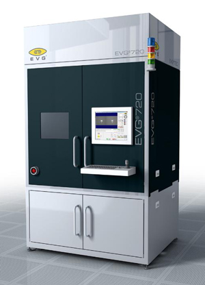
EV Group (EVG) of St Florian, Austria, a supplier of wafer bonding and lithography equipment for MEMS (microelectromechanical systems), nanotechnology and semiconductor applications, has launched the EVG 720 automated ultraviolet nanoimprint lithography (UV-NIL) system.
Providing full-field imprint lithography with an integrated soft stamp/template fabrication capability, the EVG720 enables throughputs of more than 60 wafers per hour. Capable of printing nanostructures as small as 40nm in diameter over a large area in volume production, the system is suited to use in manufacturing optics, photonics, light-emitting diodes (LEDs), microfluidics and other bioMEMS devices, as well as advanced data storage devices. Several systems have already been installed, evaluated and accepted at customer sites.

The EVG720 (the firm’s most advanced dedicated NIL system) uses a next-generation UV-NIL process designed specifically to address the needs of high-volume manufacturing (HVM). It provides a combination of high throughput, ease of use and high resolution, enabling volume manufacturing of nanoscale structures at what is claimed to be the lowest cost of ownership (CoO). EVG says that its UV-NIL solutions (including the EVG720) are designed to work with a wide variety of resist materials. This open materials platform approach provides users a high degree of flexibility and process customization, says the firm.
In addition, the EVG720 has an integrated stamp replication capability, which minimizes tool footprint and avoids increased capital equipment costs associated with stand-alone replication systems. EVG’s soft working stamps have optimized releasing properties that extend the life of the stamp and enable what is claimed to be ideal imprint results on both flat and rough substrates. Traditional stamps wear down quickly or require additional surface treatment after each imprint and result in increased defectivity on the substrate, which leads to yield loss as well as increased costs from continuous replacement.
The EVG720 platform is based on nearly 20 years of experience with more than 100 UV-based imprint lithography systems in the field, states business development manager Gerald Kreindl. “We recognize that a one-size-fits-all approach to NIL cannot address every customer’s unique manufacturing requirements, which is why EV Group has created a complete NIL solutions portfolio that encompasses all widely accepted imprint techniques: UV-NIL, hot embossing, micro contact printing, step-and-repeat, full-field, and roll-to-roll imprint,” he adds. “In addition, we are continuously working to improve the imprint lithography infrastructure by collaborating with companies and research organizations throughout the imprint lithography supply chain.”
At the SEMICON Japan show in the Makuhari Messe International Convention Complex, Chiba, Japan (4-6 December), EVG is exhibiting in booth #4B-207. Also, during the Exhibitor Seminar on 4 December at the International Conference Halls (Room 103) the firm is presenting ‘EVG's HVM solution updates for automotive and smart phone applications’. In addition, at the ‘Proposals to the Assembly Technologies to Drive 3D-IC’ session on 6 December at the TechStage West (Hall 1), Masaya Kawano, head of technology Japan/applications engineer for the Technology Division of EV Group Japan, is presenting ‘Latest wafer bonders which drive 3D-IC technology’.


