Purdue and Harvard universities have produced stacked nanowire (NW) transistors with increased drive current and maximum transconductance. The results were presented on Wednesday 12 December at the International Electron Devices Meeting (IEDM 2012) in San Francisco [J.J. Gu, X.W. Wang et al, IEDM 2012, session 23.7].
Since the nanowire transistors already have 'three dimensional' (3D) wrap-around gates, the extension into stacking has been labeled '4D electronics'. Further, in view of the time of year, it is amusing to note that the appearance of the transistor cross-section is in the stylized shape of a Christmas tree (Figure 1).
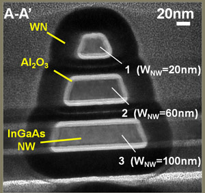
Figure 1: Transmission electron micrograph of the 4D transistor cross-section.
The researchers have built on their previous work with transistors produced using indium gallium arsenide (InGaAs) NW channels with the 'gate all-around' (GAA). InGaAs is a high-mobility III-V semiconductor compound that could power future low-power logic and radio frequency (RF) devices. The Christmas-tree effect is due to the diameter of the nanowires in the upper layers being smaller than in layers below.
The epitaxial layers of III-V material were grown on semi-insulating indium phosphide (SI InP) substrates using molecular beam epitaxy (Figure 2.1). The source/drain regions were defined using a silicon implant at two energies designed to drive the donor atoms to give a spread of depths uniformly contacting all three nanowire channels (Figure 2.2).
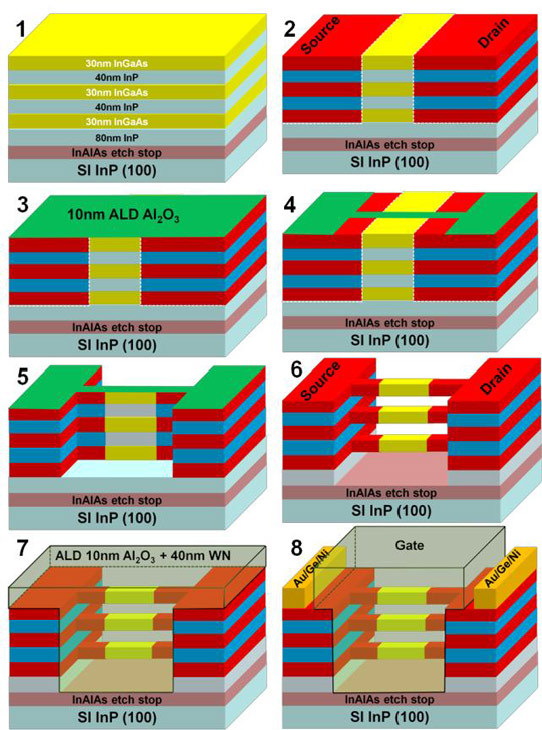
Figure 2: Schematic diagram of key process steps in the fabrication of III-V 4D transistors with 3 layers of InGaAs NWs stacked vertically.
The nanowires were formed by first reactive ion etching fins in the epitaxial material, using aluminium oxide (Al2O3) as a mask (Figures 2.3-5). The Al2O3 was applied using atomic layer deposition (ALD). The hard mask material was chosen since it does not re-deposit during the etch process, unlike electron-beam lithography resist. Also, a new etch chemistry of chlorine/oxygen, rather than the usual boron trichloride, aimed to increase the etch rate and improve quality in terms of smoother sidewalls.
The lateral etch needed to separate the InGaAs nanowires was achieved through a hydrochloric acid solution based process that removed the intervening InP material (Figure 2.6).
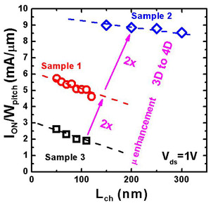
Figure 3: Benchmarking on-current (ION) normalized with respect to the maximum pitch of the nanowires in a stack (Wpitch) for new 3D, 4D and old 3D transistors (samples 1-3, respectively), indicating the benefit of EOT scaling, mobility enhancement and vertical NW stacking from 3D to 4D integration.
For the 4D structures (with larger EOT ~4.5nm), the main benefits were increased on-current (Figure 3) and maximum transconductance (Figure 4).
The all-around gate 'stack' was achieved through ALD coating of 10nm Al2O3 and conformal ALD of tungsten nitride (WN) to give the gate electrode (Figure 2.7). The source/drain electrodes were then applied (Figure 2.8).
The researchers compared the '4D' structure (3x4 NW) with '3D' single-layer 1x4 NW GAA transistors. The '1x4' consists of four lateral nanowires on the same level grouped together as transistors and '3x4' consists of 12 NWs in all with 4 NWs each in 3 layers. The researchers also compared the transistors with the group's previous 3D devices reported at IEDM in 2011. Transistors with 2x4 NWs were also produced for some of their many measurements.
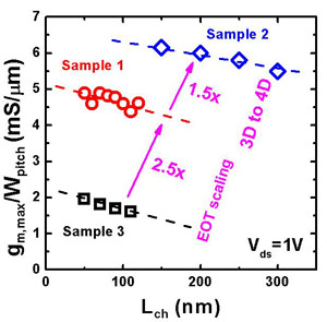
Figure 4: Benchmarking maximum transconductance (gm) per Wpitch for the same devices as Figure 3.
The new 3D devices benefited from smaller equivalent oxide thickness (EOT, 2.2nm versus 4.5nm for older device given by 5nm and 10nm of Al2O3, respectively) of the gate-insulating Al2O3 dielectric, leading to improvement in performance with respect to short-channel effects such as much reduced drain-induced barrier lowering (~50mV/V), subthreshold swing (~94mV/decade), and threshold voltage stability over different channel lengths (~-0.25V).
Although there are possibilities for thinner EOTs for both the 3D and 4D devices, there is a potential penalty in terms of increased gate leakage current. This was seen with the new 3D device.


