University of California,Santa Barbara(UCSB)has demonstrated for the first time nonpolar m-plane(10-10)nitride semiconductor vertical-cavity surface-emitting laser(VCSEL)diodes[Casey Holder et al,Appl.Phys.Express,vol5,p092104,2012].
The VCSEL structure is attractive based on its generally lower threshold current,single-longitudinal mode operation,wafer-level testing,circular and low-divergence output beams,and the ability to form densely packed,two-dimensional arrays.Until recently,VCSEL development has been focused on arsenide and phosphide compound semiconductor material systems.
Producing VCSELs in nitride semiconductor materials would yield shorter-wavelength devices.Already,c-plane violet and blue nitride VCSELs have been produced that emit in continuous-wave(cw)operation at room temperature.The more challenging green part of the spectrum has been achieved with pulsed operation at room temperature.These shorter-wavelength devices could find application in displays,high-density optical data storage,high-resolution printing,and biosensing.
Nitride semiconductor materials have large polarization fields that arise both spontaneously and through strain-dependent effects on the crystal structure.These fields reduce light emission efficiency,for example by related electric fields reducing the overlap between electrons and holes flowing through the device.
In the m-plane crystal orientation,these fields are perpendicular to the current path and hence avoid the overlap problem.However,m-plane material epitaxial growth is less established than c-plane,which has been developed intensely for the past two decades.This means that m-plane nitrides will tend to have higher defect levels,and defects reduce light-emission efficiency.
The material for the VCSELs was grown using atmospheric-pressure metal-organic chemical vapor deposition(AP-MOCVD)on Mitsubishi Chemical free-standing m-plane gallium nitride(GaN)offcut~1°in the negative c-direction(Figure 1).The active region consisted of five 7nm 10%-indium gallium nitride(InGaN)wells with 5nm GaN barriers.The electron-blocking layer consisted of 15nm p-type 20%-aluminium gallium nitride(p-AlGaN).

Figure 1:Cross-sectional schematic of nonpolar m-plane GaN VCSEL with flip-chip design and dielectric mirrors.
To enable separation of the substrate from the device layers,a sacrificial region of three 7nm 12%-InGaN wells with 5nm GaN barriers was embedded in the n-GaN buffer region.This region was used to create photoelectrons during a selective chemical etch process.Also,in the n-GaN buffer,15nm of 30%-AlGaN region was placed~50nm above the sacrificial region to define the 7.5-wavelength cavity and to prevent holes from the etch process reaching the sidewalls of the device.
The device regions were created with a mesa etch that was then covered with silicon nitride to protect the active-region sidewalls during the photoelectochemical(PEC)etch removal of the substrate.Current apertures with a diameter of 7-10??m were also defined in the SiN material.Indium tin oxide(ITO)transparent conductor(50nm thick,or about a quarter of a wavelength)was applied to the p-GaN top layer using electron cyclotron resonance(ECR)sputtering.
The metal ring p-contact was followed by dielectric layers of silicon dioxide and tantalum pentoxide to create a 13-period distributed Bragg reflector(SiO2/Ta2O5 DBR).
The PEC was prepared with a second mesa etch to expose the sacrificial undercut layer.The sample was flip-bonded to a gold-coated sapphire submount.A 405nm laser light source was used to create photoelectrons in the sacrificial layer to allow selective etching during exposure to potassium hydroxide(KOH)solution,removing the free-standing GaN substrate.
A metal ring n-contact was then formed,aligned with the p-contact aperture.A further PEC used the n-AlGaN layer as etch stop.The n-aperture was then coated with a 10-period SiO2/Ta2O5 DBR.
When operated,the VCSELs tend to have bright spots smaller than the full aperture diameter,which could be due to inhomogeneity in the cavity as a result of interface roughness or local cavity-length variations.This effect has been seen in other nitride-based VCSELs.Under pulsed operation(30nsecs,0.03%duty cycle),the peak output was 19.5??W with a threshold current of 70mA.

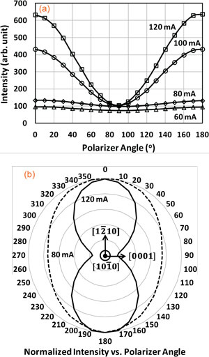
Figure 2:(a)Normalized light intensity versus polarizer angle at various currents above and below threshold.(b)Normalized light intensity versus polarizer angle well above and near threshold,plotted in radial coordinates.
"The high threshold current may be due to excessive optical loss in the cavity or leakage currents caused by cracking during the bonding process,"the researchers comment.The team is investigating how to reduce the optical loss of the cavity and has alternate designs that would reduce the parameter to 30%of its present value.
Spectral analysis with 0.3%-duty-cycle pulse operation at 100mA current gave a single peak at 411.9nm wavelength with a full-width half maximum(FWHM)of 0.25nm,which is close to the resolution limit of the measuring equipment.The distance between cavity modes is estimated to be 15nm,so a FWHM of 0.25nm gives only one mode within the gain bandwidth.
The polarization ratio of the emitted light increased with current.In the sequence 60mA,80mA,100mA and 120mA,the ratios were 0.13,0.15,0.62 and 0.72,respectively.The researchers point out that their measurements were carried out on-wafer with no special measures to eliminate spontaneous emission or light scattering.They estimate that at 120mA the spontaneous emission is around 25%of the total.
"Higher stimulated emission power and more sophisticated measurements will result in a significant increase in the polarization ratio,as spontaneous emission becomes a smaller fraction of the total light collected and collection of scattered light is reduced,"they write.
The laser emission is found to polarize along the[1-210]a-direction of the underlying wurtzite crystal structure.The researchers comment:"This is in agreement with observations of anisotropic gain in edge-emitting nonpolar GaN lasers and is believed to be the first observation of polarization locking in GaN VCSELs.This unique feature could be used to fabricate arrays of GaN VCSELs which are inherently polarization-locked and may be attractive for a variety of applications,including displays,sensors,picoprojectors,coherent detection systems,and communications."
VCSELs produced using c-plane materials have random polarization of emitted light modes.
