An international research team has been exploring the role of gate oxide border traps in devices being developed for future electronics.The researchers presented their results at the 2012 International Electron Devices Meeting[D.Lin et al,IEDM 2012,session 28.3]in San Francisco.The work was carried out at the IMEC development center in Belgium,along with Globalfoundries and Stanford University in the USA.IMEC also worked with key partners in its core CMOS technology program:Intel,Micron,Panasonic,Samsung,TSMC,Elpida,SK Hynix,Fujitsu,Toshiba/Sandisk,and Sony.
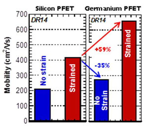
IMEC has been developing germanium(Ge)p-channel devices on 75%localized strain-relaxed buffers of silicon germanium(SiGe).This boosted mobility by 59%compared with strained silicon buffers(Figure 1).The team studied Ge Fin field-effect transistors(FETs)that were created using a silicon replacement process that the researchers see as having potential for 10nm and 7nm transistor nodes.The industry hopes that high-mobility channels,made from Ge for pMOS and III-V materials for nMOS,will lead to faster devices that can also be configured to operate on lower power for mobile applications.

Figure 1:Comparison of mobility in unstrained and strained Si and Ge p-FinFETs.Unstrained Ge shows degraded mobility with respect to strained Si.Strained Ge can improve pFET mobility by 59%.
Much work on high-mobility transistors has recently focused on traps at the interface between the gate oxide insulation and the channel.These traps introduce adverse delay effects on device performance.IMEC says this work means that this problem now appears to be contained.
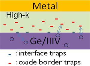
The new work by IMEC et al explored the adverse impact of oxide border traps in the oxide insulator of the metal-oxide-semiconductor(MOS)gate stack(Figure 2).Shallow,fast oxide traps have been linked to frequency-dependent transconductance effects in non-silicon MOSFETs.Such frequency dependence can pose significant problems for circuit design using the new transistors.

Figure 2:Without a highly insulating interfacial blocking layer(e.g.SiO2),carriers in the channel can directly interact with border traps(BT)in the high-k dielectric.
The researchers also mapped out slower traps using trap spectroscopy by charge injection and sensing(TSCIS).These traps cause threshold voltages(VT)to drift,creating problems with predicting how a circuit will perform over time.Further,the overdrive voltages(VON-VT)for III-V(255mV)and Ge-based(212mV)transistors are expected to be about a factor of three smaller than for present silicon-based devices,making threshold drift a much more significant problem.The lower overdrive without drift is targeted by the International Technology Roadmap for Semiconductors(ITRS)because it allows lower-voltage/power operation.
The researchers write:"This study raises the urgent issues of border traps and the need for engineering workarounds.Fundamental understandings on the nature and formation of these traps are required for long-term solutions."
Aaron Thean,director of the logic program at IMEC,adds:"With each new technology generation,challenges are immense.And IMEC has always come up with solutions to extend Moore's law.Moving on towards the 14nm node and beyond,we are confident that,again,we will find solutions for the challenges that lie ahead.We are looking into high-mobility channel materials,such as Ge and III-V compounds,focusing on two main challenges:namely,how to implement non-Si materials into the device architecture;and how to overcome some of the fundamental physics of the gate stack related to passivation."


