Researchers in France have developed a monolithic metal-organic vapor phase epitaxy (MOVPE) process for growing indium gallium nitride (InGaN) light-emitting diodes (LEDs) with a multiple quantum well (MQW) light converter [Benjamin Damilano et al, Appl. Phys. Express, vol6, p092105, 2013]. The research involved Centre de Recherche sur l'Hétéro-Epitaxie et ses Applications–Centre National de la Recherche Scientifique (CRHEA-CNRS) and University of Nice Sophia-Antipolis.
Presently, standard commercial white light LEDs use phosphor layers to convert short-wavelength light from InGaN LEDs into something that the eye will see as being an approximation to 'white'. Phosphors make the production process more complicated and costly. Technical difficulties include reliability problems, and degradation of the color balance over time and due to temperature stress.
An alternative approach is to use the short-wavelength LED as a pump for photoluminescence from an InGaN MQW structure that emits longer wavelengths. The researchers have previously developed such structures, but the production process used molecular beam epitaxy (MBE), sometimes in combination with MOVPE. Commercial production of InGaN LEDs is usually based on MOVPE.
A problem with MOVPE is that it uses higher growth temperatures than MBE that can degrade the high-indium-content InGaN needed for longer wavelengths. The researchers developed an MOVPE process that uses a lower temperature but does not degrade the pump LED performance.
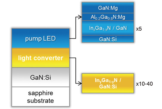
The nitride semiconductor layers (Figure 1) were grown on commercial n-type silicon-doped gallium nitride (GaN:Si) on sapphire using MOVPE. First, a 0.5μm layer of GaN:Si was grown at 1080°C. The temperature was reduced to 715-780°C for the InyGa1-yN layers in the light-conversion MQW.

Figure 1: Structure of monolithic LED with light converter.
The researchers found that they were able to produce light conversion from violet into blue to red (490-605nm). Although spectral purity is often desired in colored LEDs, for white light sources with good color rendering indices (CRIs) the researchers wanted broad photoluminescence peaks. Such broadening can occur due to fluctuations in the InGaN alloy composition or from quantum well interface roughness. Measured photoluminescence (PL) spectra of wafers with just the light converter MQW structure showed small intensity oscillations due to interference effects from the cavity formed by the GaN layers sandwiched between sapphire and air.
Four pump/converter structures were produced with varying light-converter regions (Table 1). The pump LED consisted of a 20nm GaN:Si n-contact, 5x(1.4nm In0.1Ga0.9N/9nm GaN) MQW, 15nm Al0.2Ga0.8N electron-blocking layer, and 150nm GaN:Mg p-contact. The InGaN of the pump MQW was grown at 800°C.
Table 1: Structures of the different light converter sections.
Sample A B C D Number of QWs 20 10 40 40 InyGa1-yN thickness (nm) 1.6 3.4 3.1 3.1 In composition (y) 0.26 0.18 0.22 0.28 GaN:Si barrier thickness (nm) 21 18 18 18
The standard growth temperature for GaN and AlGaN of ~1080°C was found to result in poor performance. In particular, the light-converter regions showed signs of indium metal clustering. Thus, a lower temperature of 970°C was adopted while, at the same time, the p-doping effect of magnesium (Mg) had to be re-optimized for the lower growth temperature.
The samples were used to produce on-wafer LEDs by scratching the top surface with a diamond tip, exposing the GaN:Si layer of the pump LED. The electrical contacts with the GaN:Si and GaN:Mg layers were made with indium metal.
Despite the non-standard growth, the researchers were able to produce violet LEDs with ~2mW output power at 20mA, similar to values obtained for devices grown at higher temperatures. The peak of the pump's emission spectrum was around 400nm.
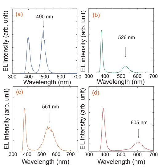
The effect of the light converters (Figure 2) was to add peaks at 490nm (sample A), 526nm (B), 551nm (C), and 605nm (D). The researchers describe these devices as emitting blue, green, yellow-green, and white-orange light, respectively.

Figure 2: (a)–(d) RT EL spectra under continuous-wave conditions at a current of 20mA corresponding to samples A–D.
The fractions of the long-wavelength peak relative to the total electroluminescence intensity were, in order, 60%, 55%, 70%, and 43%. Despite the expected degradation in performance from increased indium content, sample C shows an increased fraction of the longer-wavelength peak. The researchers ascribe this to greater absorption from the use of 40 quantum wells rather than the 10 of sample B. Another factor may be variations in the peak wavelength of the pump LED, but other studies suggest that the effect of this should be small.
The 50mA luminous powers for samples A-D were 86mlm, 264mlm, 67mlm, and 5mlm, respectively. Since lumens corrects for the eye's sensitivity to light of different wavelengths with a maximum in the green part of the spectrum (683lm/W at 555nm), the optimum luminous power is for sample B. Previous attempts to use a pump/light-converter structure have produced 200mlm for material grown using a mix of MOVPE (converter) and MBE (pump). Sample B beats this previous achievement by 32%.
In terms of chromatic coordinates, sample D is close to that of a black-body of temperature 2100K. This tint is between warm white and candlelight.
The researchers believe the work could be extended to include a range of emissions from the converter section. This could be used to improve the CRI to bring it in line with a white light source at various color temperatures.


