IBM is working with scientists at ETH Zurich to demonstrate the first-ever direct mapping of the formation of a persistent spin helix in a semiconductor.This has implications for the use of electron spins for storing,transporting and processing information.
It has previously not been confirmed that electron spins possessed the capability to preserve the encoded information long enough before rotating.The scientists from IBM Research and the Solid State Physics Laboratory at ETH Zurich demonstrated that synchronising electrons extends the spin lifetime of the electron by 30 times to 1.1 nanoseconds.This is the same time it takes for an existing 1GHz processor to cycle.
"This new understanding in spintronics not only gives scientists unprecedented control over the magnetic movements inside devices but also opens new possibilities for creating more energy efficient electronics,"said IBM.
Spintronics is interesting because it provides an alternative to the traditional means of processing data in electronic devices by the electrical charge of electrons.It is thought this could break through the limitations imposed by semiconductor dimensions shrinking to the point where the flow of electrons can no longer be controlled.
IBM scientists used ultra short laser pulses to monitor the evolution of thousands of electron spins that were created simultaneously in a very small spot.
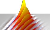
Atypically,where such spins would randomly rotate and quickly loose their orientation,for the first time,the scientists could observe how these spins arrange neatly into a regular stripe-like pattern,the so-called persistent spin helix.
Transferring spin electronics from the laboratory to the market still remains a major challenge.
Spintronics research takes place at very low temperatures at which electron spins interact minimally with the environment.In the case of this particular research IBM scientists worked at 40 Kelvin(-233 C,-387 F).
The concept of locking the spin rotation was originally proposed in theory back in 2003 and since that time some experiments have even found indications of such locking,but until now it had never been directly observed.
IBM scientists imaged the synchronous'waltz'of the electron spins by using a time-resolved scanning microscope technique.
The synchronisation of the electron spin rotation made it possible to observe the spins travel for more than 10μm,increasing the possibility to use the spin for processing logical operations,both fast and energy-efficiently.
The reason for the synchronous spin motion is a carefully engineered spin-orbit interaction,a physical mechanism that couples the spin with the motion of the electron.
The semiconductor material called gallium arsenide(GaAs)was produced by scientists at ETH Zurich who are known as world-experts in growing ultra-clean and atomically precise semiconductor structures.GaAs is a III/V semiconductor commonly used in the manufacture of devices such as integrated circuits,infrared light-emitting diodes and highly efficient solar cells.


