The Millimeter-Wave Electronics Group of the Swiss Federal Institute of Technology(ETH)Zurich has been exploring the use of Teflon amorphous fluoropolymer(AF)as an interlayer dielectric for
III-V double heterostructure bipolar transistors(DHBT)[Ralf Flückiger et al,IEEE Electron Device Letters,published online 5 July 2012].
Teflon is attractive as an interlayer dielectric(ILD)due to its relatively low dielectric constant(1.9),giving low interconnect delays.Although some applications have been found,"to date,the use of Teflon AF ILDs in high-speed transistor technologies has never been reported,"the researchers write.
Most work on III-V transistors uses benzocyclobutene(BCB)as the ILD of choice.BCB's dielectric constant at 2.7 is significantly higher than Teflon's.Teflon's dissipation factor is also 4x lower,and can be cured at lower temperatures than BCB's more than 250°C.High-temperature curing can degrade base contact performance.
The researchers used Teflon with indium phosphide/gallium arsenide antimonide(InP/GaAsSb)devices,but they believe that the approach is equally applicable to gallium indium arsenide HBTs and InP-based high-electron-mobility transistors(HEMTs).
The researchers compared their devices with air-bridge samples(i.e.with no ILD),which give the lowest dielectric constant of 1.However,air-bridge connections suffer from problems such as sagging,which raise difficulties for mass manufacturing robust,reliable devices.

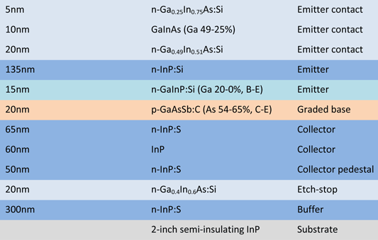
Figure 1:Epitaxial structure of InP/GaAsSb DHBTs.
The epitaxial layers for the ETH devices(Figure 1)were grown using metal-organic vapor phase epitaxy(MOVPE).Triple mesa structures were formed(Figure 2 inset).The Teflon interlayer dielectric was spin-coated in perfluorinated solution onto the device and then baked at temperatures that increased in three steps to 110°C(1 min),165°C(15 min)and 180°C(30 min).The resulting cured 2.7μm layer was etched back to 1.7μm,exposing emitter,base and collector contact posts for final interconnect metallization.

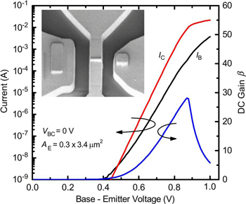
Figure 2:Gummel characteristics for a 0.3μm x 3.4μm DHBT measured with VBC=0V.The DC gain as a function of VBE is also plotted.(Inset)SEM micrograph of a completed transistor with interconnects on Teflon.
The researchers found that their technique provided sufficient planarization and enough dielectric material was left to reliably prevent short-circuiting between device terminals.The researchers believe that multiple layers and higher baking temperatures could improve the planarization,if necessary.
The team has also performed experiments where up to six layers of the Teflon were deposited,giving a stack thickness of 16.8μm.The researchers comment:"These findings suggest that monolithic microwave ICs(MMICs)with multiple metallization layers are feasible with this technology.Previous work by others has further established that Teflon AF films are fully compatible with submicrometer IC processing."
The DC current gain of the resulting device was 28 at 0.87V base-emitter and 0V base-collector biases.The common emitter breakdown voltage at 1kA/cm2 current density was 5.1V.
Extrapolated cut-off(fT)and maximum oscillation(fMAX)frequencies were 362GHz(366GHz by Gummel's method)and 450GHz,respectively,at 1.6V collector-emitter bias and with 8.9mA collector current when corrected for pad parasitics('de-embedded').The peaking of the two characteristics occurred simultaneously at the given bias condition.
A side-by-side comparison of slightly different epitaxial devices with Teflon planarization and with air-bridge interconnects showed about 3%reduction in frequency performance for Teflon(325GHz/330GHz fT/fMAX).The reduction of frequency performance was compensated by a 4%improvement in DC gain.
The researchers conclude:"We consider the present developments significant in terms of demonstrating a much needed low-temperature alternative to high-temperature BCB processes,with the added advantage of providing a high-quality interconnect dielectric medium for the realization of millimeter-and submillimeter-wave ICs."


