Institute of Electronic, Microelectronic and Nanotechnology (IEMN) in France and EpiGaN nv in Belgium have claimed a record combination of specific on-resistance and breakdown voltage for a double heterostructure field-effect transistor (DHFET) using a gallium nitride (GaN) channel and aluminium nitride (AlN) barrier on silicon (Si) substrate [Nicolas Herbecq et al, Appl. Phys. Express, vol7, p034103, 2014].
The team tackled leakage problems from substrate conduction by locally removing silicon from beneath critical parts of the device to achieve a breakdown voltage of 1.9kV with a specific on-resistance of 1.6mΩ-cm2.
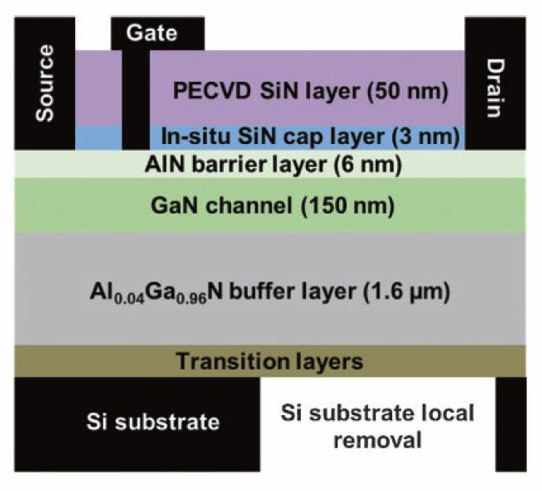
The epitaxial nitride semiconductor layers for the transistor (Figure 1) were grown by metal-organic chemical vapor deposition (MOCVD) on 4-inch silicon (111) substrates. The 3nm silicon nitride (SiN) layer produced in-situ in the MOCVD reaction chamber provided early passivation and also prevented strain relaxation and increased surface robustness.

Figure 1: Schematic of AlN/GaN/AlGaN DHFET with local substrate removal.
The use of an AlN barrier gave a high electron carrier density of 2.3x10¹³/cm2 with mobility 990cm2/V-s. The sheet resistance was 280Ω/square. The device included an AlGaN back-barrier/buffer to further improve breakdown performance by reducing leakage.
The transistor fabrication began with titanium/aluminium/nickel/gold ohmic contact formation on the AlN layer after etching through the cap layer. The contact metals were annealed at 875°C. The devices were isolated with nitrogen implantation.
Fabrication continued with plasma-enhance chemical vapor deposition (PECVD) of 50nm SiN. The gate was formed by etching through the SiN to the AlN layer with a low-damage low-power sulfur hexafluoride (SF6) plasma and then depositing nickel/gold as the gate metal. The gate was 1.5μm long and 50μm wide. The gate-source spacing was 1.5μm. The distance between the gate and drain electrodes varied from 2μm up to 15μm. The gate was extended 0.75μm in the drain direction to create a field-plate.
The backside processing involved thinning and polishing the Si substrate down to 230μm, followed by local deep reactive-ion etch to the AlGaN buffer layer using the ‘Bosch process’ on a Surface Technology Systems tool. The Bosch technique involves a sequence of passivation and etch steps, which results in reproducible vertical walls and allows high aspect ratios to be achieved.
The local etch removed material around the drain contact. One potential drawback of the removal of material is degradation of thermal dissipation. The trenches were 20μm wide, extending over the gate-drain region.
The DC performance of the devices with local backside etching did show reduced performance in terms of maximum drain current and peak transconductance. In devices with 15μm gate-drain spacing, the maximum drain current without local Si removal was 0.7A/mm. This was reduced 28% to 0.5A/mm with Si removal. These values corresponded to specific on-resistances of 1.3mΩ-cm2 and 1.6mΩ-cm2 for the devices without and with Si removal, respectively. The researchers attributed the difference to self-heating effects due to inadequate thermal dissipation with local Si removal. High temperature reduces channel mobility in GaN-based devices.
Both devices had a low off-state current less than 10μA/mm, despite the lack of gate insulation.
Three-terminal breakdown voltage measurements were carried out in a ‘deep pinch-off’ state with the gate at -5V. The breakdown current of 1mA/mm was used. The breakdown voltage for both types of device increased linearly with gate-drain distances up to 8μm. Beyond 8μm, the breakdown for devices without substrate removal saturated at around 750V. The limitation is attributed to the electric field reaching down through the thin buffer (~1.8μm) and effecting conduction through the substrate.
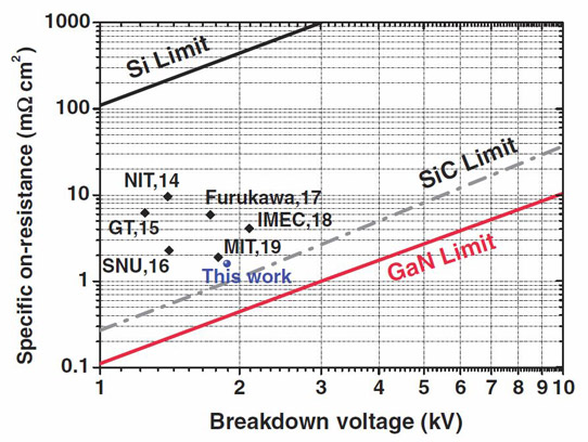
With local substrate removal, the breakdown voltage continued to increase linearly to 1.9kV with a gate-drain distance of 15μm. The device compares well with ‘state-of-the-art’ in terms of high breakdown voltage and low specific on-resistance (Figure 2).

Figure 2: Benchmarking of specific on-resistance versus breakdown voltage of GaN-on-Si transistors rated above 1kV.
The researchers believe the technique could be used to extend the gate-drain spacing to ~30μm, allowing 3kV blocking to be reached with less than 5mΩ-cm2 specific on-resistance. Gate insulation would reduce leakage further. The team also suggests that a thick dielectric trench fill with, for example, AlN, could reduce self-heating effects.


